SLVSD01B September 2015 – May 2019 TPS57140-EP
PRODUCTION DATA.
- 1 Features
- 2 Applications
- 3 Description
- 4 Revision History
- 5 Pin Configuration and Functions
- 6 Specifications
-
7 Detailed Description
- 7.1 Overview
- 7.2 Functional Block Diagram
- 7.3
Feature Description
- 7.3.1 Fixed Frequency PWM Control
- 7.3.2 Slope-Compensation Output Current
- 7.3.3 Bootstrap Voltage (Boot)
- 7.3.4 Low-Dropout Operation
- 7.3.5 Error Amplifier
- 7.3.6 Voltage Reference
- 7.3.7 Adjusting the Output Voltage
- 7.3.8 Enable and Adjusting UVLO
- 7.3.9 Slow-Start or Tracking Pin (SS/TR)
- 7.3.10 Overload Recovery Circuit
- 7.3.11 Constant Switching Frequency and Timing Resistor (RT/CLK Pin)
- 7.3.12 Overcurrent Protection and Frequency Shift
- 7.3.13 Selecting the Switching Frequency
- 7.3.14 How to Interface to RT/CLK Pin
- 7.3.15 Power Good (PWRGD Pin)
- 7.3.16 Overvoltage Transient Protection (OVTP)
- 7.3.17 Thermal Shutdown
- 7.3.18 Small-Signal Model for Loop Response
- 7.3.19 Simple Small-Signal Model for Peak-Current-Mode Control
- 7.3.20 Small-Signal Model for Frequency Compensation
- 7.4 Device Functional Modes
-
8 Application and Implementation
- 8.1 Application Information
- 8.2
Typical Application
- 8.2.1 Design Requirements
- 8.2.2
Detailed Design Procedure
- 8.2.2.1 Selecting the Switching Frequency
- 8.2.2.2 Output Inductor Selection (LO)
- 8.2.2.3 Output Capacitor
- 8.2.2.4 Catch Diode
- 8.2.2.5 Input Capacitor
- 8.2.2.6 Slow-Start Capacitor
- 8.2.2.7 Bootstrap Capacitor Selection
- 8.2.2.8 UVLO Set Point
- 8.2.2.9 Output Voltage and Feedback Resistors Selection
- 8.2.2.10 Compensation
- 8.2.3 Application Curves
- 9 Power Supply Recommendations
- 10Layout
- 11Device and Documentation Support
- 12Mechanical, Packaging, and Orderable Information
Package Options
Mechanical Data (Package|Pins)
- DRC|10
Thermal pad, mechanical data (Package|Pins)
- DRC|10
Orderable Information
7.3.9 Slow-Start or Tracking Pin (SS/TR)
The TPS57140-EP effectively uses the lower voltage of the internal voltage reference or the SS/TR pin voltage as the power-supply reference voltage and regulates the output accordingly. A capacitor on the SS/TR pin to ground implements a slow-start time. The TPS57140-EP has an internal pullup current source of 2 μA that charges the external slow-start capacitor. The calculations for the slow-start (Equation 6) show the time (10% to 90%). The voltage reference (VREF) is 0.8 V and the slow-start current (ISS) is 2 μA. The slow-start capacitor should remain lower than 0.47 μF and greater than 0.47 nF.

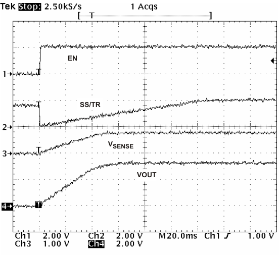
At power up, the TPS57140-EP does not start switching until the slow-start pin discharges to <40 mV; to ensure proper power up, see Figure 31.
During normal operation, the TPS57140-EP stops switching and the SS/TR must discharge to 40 mV when the VIN UVLO is exceeded, EN pin is pulled below 1.2 V, or a thermal shutdown event occurs.
The VSENSE voltage follows the SS/TR pin voltage with a 45-mV offset up to 85% of the internal voltage reference. When the SS/TR voltage is >85% of the internal reference voltage, the offset increases as the effective system reference transitions from the SS/TR voltage to the internal voltage reference (see Figure 24). The SS/TR voltage ramps linearly until clamped at 1.7 V.
 Figure 31. Operation of SS/TR Pin When Starting