SLVSD01B September 2015 – May 2019 TPS57140-EP
PRODUCTION DATA.
- 1 Features
- 2 Applications
- 3 Description
- 4 Revision History
- 5 Pin Configuration and Functions
- 6 Specifications
-
7 Detailed Description
- 7.1 Overview
- 7.2 Functional Block Diagram
- 7.3
Feature Description
- 7.3.1 Fixed Frequency PWM Control
- 7.3.2 Slope-Compensation Output Current
- 7.3.3 Bootstrap Voltage (Boot)
- 7.3.4 Low-Dropout Operation
- 7.3.5 Error Amplifier
- 7.3.6 Voltage Reference
- 7.3.7 Adjusting the Output Voltage
- 7.3.8 Enable and Adjusting UVLO
- 7.3.9 Slow-Start or Tracking Pin (SS/TR)
- 7.3.10 Overload Recovery Circuit
- 7.3.11 Constant Switching Frequency and Timing Resistor (RT/CLK Pin)
- 7.3.12 Overcurrent Protection and Frequency Shift
- 7.3.13 Selecting the Switching Frequency
- 7.3.14 How to Interface to RT/CLK Pin
- 7.3.15 Power Good (PWRGD Pin)
- 7.3.16 Overvoltage Transient Protection (OVTP)
- 7.3.17 Thermal Shutdown
- 7.3.18 Small-Signal Model for Loop Response
- 7.3.19 Simple Small-Signal Model for Peak-Current-Mode Control
- 7.3.20 Small-Signal Model for Frequency Compensation
- 7.4 Device Functional Modes
-
8 Application and Implementation
- 8.1 Application Information
- 8.2
Typical Application
- 8.2.1 Design Requirements
- 8.2.2
Detailed Design Procedure
- 8.2.2.1 Selecting the Switching Frequency
- 8.2.2.2 Output Inductor Selection (LO)
- 8.2.2.3 Output Capacitor
- 8.2.2.4 Catch Diode
- 8.2.2.5 Input Capacitor
- 8.2.2.6 Slow-Start Capacitor
- 8.2.2.7 Bootstrap Capacitor Selection
- 8.2.2.8 UVLO Set Point
- 8.2.2.9 Output Voltage and Feedback Resistors Selection
- 8.2.2.10 Compensation
- 8.2.3 Application Curves
- 9 Power Supply Recommendations
- 10Layout
- 11Device and Documentation Support
- 12Mechanical, Packaging, and Orderable Information
Package Options
Mechanical Data (Package|Pins)
- DRC|10
Thermal pad, mechanical data (Package|Pins)
- DRC|10
Orderable Information
7.3.20 Small-Signal Model for Frequency Compensation
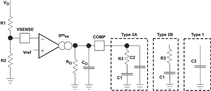
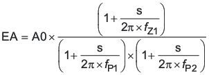
The TPS57140-EP uses a transconductance amplifier for the error amplifier and readily supports three of the commonly-used frequency compensation circuits. Figure 41 shows compensation circuits Type 2A, Type 2B, and Type 1. Type 2 circuits are most likely used in high-bandwidth power-supply designs using low-ESR output capacitors. Power-supply designs with high-ESR aluminum electrolytic or tantalum capacitors likely use the Type 1 circuit. Equation 14 and Equation 15 show how to relate the frequency response of the amplifier to the small-signal model in Figure 41. Modeling of the open-loop gain and bandwidth uses the RO and CO shown in Figure 41. See Application and Implementation for a design example using a Type 2A network with a low-ESR output capacitor.
Equation 14 through Equation 23 are a reference for those who prefer to compensate using the preferred methods. Those who prefer to use a prescribed method must use the method outlined in Application and Implementation or use switched information.
 Figure 41. Types of Frequency Compensation
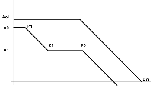
  Figure 42. Frequency Response of the Type 2A and Type 2B Frequency Compensation


