SLUSDL4 February 2020 TPS59632-Q1
PRODUCTION DATA
- 1 Features
- 2 Applications
- 3 Description
- 4 Revision History
- 5 Pin Configuration and Functions
- 6 Specifications
-
7 Detailed Description
- 7.1 Overview
- 7.2 Functional Block Diagram
- 7.3
Feature Description
- 7.3.1 PWM Operation
- 7.3.2 Current Sensing
- 7.3.3 Load-line (Droop)
- 7.3.4 Load Transients
- 7.3.5 Overshoot Reduction (OSR)
- 7.3.6 Undershoot Reduction (USR)
- 7.3.7 Autobalance Current Sharing
- 7.3.8 PWM And SKIP Signals
- 7.3.9 Bias Power (V5A, VDD, And VINTF) UVLO
- 7.3.10 Start-Up Sequence
- 7.3.11 Power Good Operation
- 7.3.12 Analog Current Monitor, IMON, And Corresponding Digital Output Current
- 7.3.13 Fault Behavior
- 7.3.14 Output Under Voltage Protection (UVP)
- 7.3.15 Output Over Voltage Protection (OVP)
- 7.3.16 Over Current Protection (OCP)
- 7.3.17 Over Current Warning
- 7.3.18 Input Voltage Limits
- 7.3.19 VID Table
- 7.4 User Selections
- 7.5 I2C Interface Operation
- 7.6 I2C Register Maps
-
8 Applications and Implementation
- 8.1 Application Information
- 8.2
Typical Application
- 8.2.1
3-Phase D-CAP+™, Step-Down Application
- 8.2.1.1 Design Requirements
- 8.2.1.2
Detailed Design Procedure
- 8.2.1.2.1 Step 1: Select Switching Frequency
- 8.2.1.2.2 Step 2: Set The Slew Rate
- 8.2.1.2.3 Step 3: Set The I2C Address
- 8.2.1.2.4 Step 4: Determine Inductor Value And Choose Inductor
- 8.2.1.2.5 Step 5: Current Sensing Resistance
- 8.2.1.2.6 Step 6: Select Over Current Protection (OCP) Setting
- 8.2.1.2.7 Step 7: Current Monitor (IMON) Setting
- 8.2.1.2.8 Step 8: Set the Load-Line Slope
- 8.2.1.2.9 Step 9: Voltage Feedback Resistor Calculation
- 8.2.1.2.10 Step 10: Ramp Compensation Selection
- 8.2.1.2.11 Step 11 Overshoot Reduction (OSR) selection
- 8.2.1.2.12 Step 12: Undershoot Reduction (USR) selection
- 8.2.1.2.13 Step 13: Loop Compensation
- 8.2.1.3 Application Performance Plots
- 8.2.1
3-Phase D-CAP+™, Step-Down Application
- 9 Power Supply Recommendations
- 10Layout
- 11Device and Documentation Support
- 12Mechanical, Packaging, and Orderable Information
Package Options
Mechanical Data (Package|Pins)
- RHB|32
Thermal pad, mechanical data (Package|Pins)
- RHB|32
Orderable Information
8.2.1.2.6 Step 6: Select Over Current Protection (OCP) Setting
The OCP level is chosen such that it is 30% above the maximum load current, ICC(max). In the equation, here RCS is the current sense resistor.Equation 4. IVALLEY is the load current less half the ripple.
Equation 4. 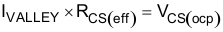
Set the OCP threshold level just greater than the calculated IVALLEY for the required OCP level. Equation 4. In this design, the minimum required OCP is 65A. Therefore, an OCP selection resistor of 56k is chosen to meet the requirement.
Table 8-4 shows the minimum OCP level for all the selection resistors.
Table 8-4 OCP Selection(1)
| SELECTION RESISTOR ROCP (kΩ) | Minimum VCS(OCP) (mV) |
|---|---|
| 20 | 3 |
| 24 | 7 |
| 30 | 11 |
| 39 | 15 |
| 56 | 21 |
| 75 | 28 |
| 100 | 36 |
| 150 | 45 |
(1) If a corresponding match is not found, then select the next higher setting.