SLVS258B November 1999 – December 2016 TPS60130 , TPS60131 , TPS60132 , TPS60133
PRODUCTION DATA.
- 1 Features
- 2 Applications
- 3 Description
- 4 Revision History
- 5 Device Options
- 6 Pin Configuration and Functions
- 7 Specifications
- 8 Parameter Measurement Information
- 9 Detailed Description
- 10Application and Implementation
- 11Power Supply Recommendations
- 12Layout
- 13Device and Documentation Support
- 14Mechanical, Packaging, and Orderable Information
Package Options
Mechanical Data (Package|Pins)
- PWP|20
Thermal pad, mechanical data (Package|Pins)
- PWP|20
Orderable Information
10 Application and Implementation
NOTE
Information in the following applications sections is not part of the TI component specification, and TI does not warrant its accuracy or completeness. TI’s customers are responsible for determining suitability of components for their purposes. Customers should validate and test their design implementation to confirm system functionality.
10.1 Application Information
The TPS6013x charge pumps provide a regulated 5-V output from a 2.7-V to 5.4-V input. They deliver a maximum load current of 300 mA or 150 mA (respectively).
10.2 Typical Applications
10.2.1 Paralleling of Two TPS6013x to Deliver 600-mA Total Output Current
Two TPS60130x devices can be connected in parallel to yield higher load currents. The circuit of Figure 23 can deliver up to 600 mA at an output voltage of 5 V.
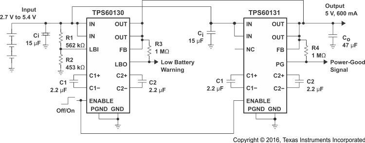 Figure 23. Paralleling of Two TPS6013x Charge Pumps
10.2.1.1 Design Requirements
The device operates over an input voltage range from 2.7 V to 5.4 V.
10.2.1.2 Detailed Design Procedure
The devices can share the output capacitors, but each one requires its own transfer capacitors and input capacitor. If both a TPS60130 and a TPS60131 are used, it is possible to monitor the battery voltage with the TPS60130 using the low battery comparator function and to supervise the output voltage with the TPS60131 using the Power Good comparator. Make the layout of the charge pumps as similar as possible, and position the output capacitor the same distance from both devices.
10.2.1.2.1 Capacitor Selection
The TPS6013x charge pump require only four external capacitors as shown in the basic application circuit. Their capacitance values and types are closely linked to the output current and output noise and ripple requirements. For lowest noise and ripple, low ESR (<0.1 Ω) capacitors must be used for input and output capacitors.
The input capacitor improves system efficiency by reducing the input impedance. It also stabilizes the input current of the power source. The input capacitor must be chosen according to the power supply used and the distance from power source to the converter IC. The input capacitor also has an impact on the output voltage ripple. The lower the ESR of the input capacitor Ci, the lower is the output ripple. TI recommends Ci be about two to four times as large as C(xF).
The output capacitor Co can be selected from 5-times to 50-times larger than C(xF), depending on the ripple tolerance. The larger Co, the lower is the output voltage ripple. Ci and Co can be either ceramic or low-ESR tantalum; aluminum capacitors are not recommended.
Generally, the flying capacitors C(xF) is the smallest. Only ceramic capacitors are recommended, due to their low ESR and because they retain their capacitance at the switching frequency. Because the device regulates the output voltage using the pulse-skip technique, a larger flying capacitor leads to a higher output voltage ripple if the size of the output capacitor is not increased. Be aware that, depending on the material used to manufacture them, ceramic capacitors might lose their capacitance over temperature. Ceramic capacitors of type X7R or X5R material keep their capacitance over temperature and voltage, whereas Z5U or Y5V-type capacitors decrease in capacitance. Table 5 lists recommended capacitor values.
Table 5. Recommended Capacitor Values
| PART | VI (V) | IO (mA) | Ci (µF) | CxF
CERAMIC (X7R) |
Co (µF) | VPP(TYP) (V) | ||
|---|---|---|---|---|---|---|---|---|
| TANTALUM | CERAMIC (X7R) | TANTALUM | CERAMIC (X7R) | |||||
| TPS60130, TPS60131 |
3.6 | 225 | — | 10 | 2.2 | 22 | 4.7 | 90 |
| — | — | 22 | 60 | |||||
| TPS60132, TPS60133 |
3.6 | 300 | — | 10 | 2.2 | 33 | 4.7 | 120 |
| — | — | 22 and 10 in parallel |
45 | |||||
| 75 | — | 4.7 | 1 | — | 10 | — | ||
| 150 | 4.7 | 2.2 | 15 | 22 | 100 | |||
| — | 4.7 | — | 22 | 90 | ||||
The TPS6013x devices are charge pumps that regulate the output voltage using pulse-skip regulation mode. The output voltage ripple is therefore dependent on the values and the ESR of the input, output and flying capacitors. The only possibility to reduce the output voltage ripple is to choose the appropriate capacitors. The lowest output voltage ripple can be achieved using ceramic capacitors because of their low ESR and their frequency characteristic.
Ceramic capacitors typically have an ESR that is more than 10 times lower than tantalum capacitors and they retain their capacitance at frequencies more than 10 times higher than tantalum. Many different tantalum capacitors act as an inductance for frequencies higher than 200 kHz. This behavior increases the output voltage ripple. Therefore, the best choice for a minimized ripple is the ceramic capacitor. For applications that do not require a higher performance in output voltage ripple, tantalum capacitors with a low ESR are a possibility for input and output capacitor, but a ceramic capacitor must be connected in parallel. Be aware that the ESR of tantalum capacitors is indirectly proportional to the physical size of the capacitor.
Table 5 is a good starting point for choosing the capacitors. If the output voltage ripple is too high for the application, it can be improved by selecting the appropriate capacitors. The first step is to increase the capacitance at the output. If the ripple is still too high, the second step would be to increase the capacitance at the input.
For the TPS60130 and TPS60131, the smallest board space can be achieved using Sprague’s 595D-series tantalum capacitors for input and output. However, high-capacitance ceramic capacitors become competitive in package size soon.
The smallest size for the lower-current devices TPS60132 and TPS60133 can be achieved using the suggested ceramic capacitors.
Table 6 lists the manufacturers of recommended capacitors. In most applications, surface-mount tantalum capacitors is the right choice. However, ceramic capacitors provide the lowest output voltage ripple due to their typically lower ESR.
Table 6. Recommended Capacitors(1)
| MANUFACTURER | PART NUMBER | CAPACITANCE | CASE SIZE | TYPE |
|---|---|---|---|---|
| Taiyo Yuden | LMK212BJ105KG−T | 1 µF | 0805 | Ceramic |
| LMK212BJ225MG−T | 2.2 µF | 0805 | Ceramic | |
| LMK316BJ475KL−T | 4.7 µF | 1206 | Ceramic | |
| LMK325BJ106MN−T | 10 µF | 1210 | Ceramic | |
| LMK432BJ226MM−T | 22 µF | 1812 | Ceramic | |
| AVX | 0805ZC105KAT2A | 1 µF | 0805 | Ceramic |
| 1206ZC225KAT2A | 2.2 µF | 1206 | Ceramic | |
| TPSC475035R0600 | 4.7 µF | Case C | Tantalum | |
| TPSC156025R0500 | 10 µF | Case C | Tantalum | |
| TPSC336010R0375 | 22 µF | Case C | Tantalum | |
| Sprague | 595D156X0016B2T | 15 µF | Case B | Tantalum |
| 595D226X0016B2T | 22 µF | Case B | Tantalum | |
| 595D336X0016B2T | 33 µF | Case B | Tantalum | |
| 595D336X0016C2T | 33 µF | Case C | Tantalum | |
| Kemet | T494C156K010AS | 15 µF | Case C | Tantalum |
| T494C226K010AS | 22 µF | Case C | Tantalum | |
| T494C336K010AS | 33 µF | Case C | Tantalum |
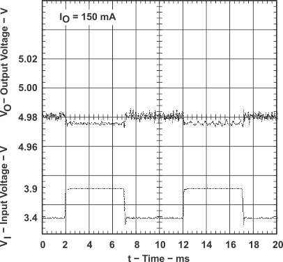
10.2.1.3 Application Curves
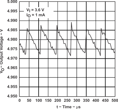
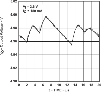
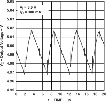
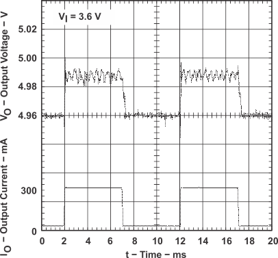
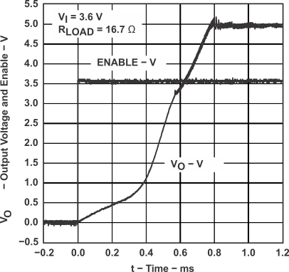
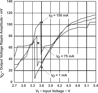
vs Input Voltage
10.2.2 TPS6013x Operated With Ultra-Low Quiescent Current
Because the output of the TPS6013x is isolated from the input when the devices are disabled, and because the internal resistive divider is disconnected in shutdown, an ultra-low quiescent current mode can be implemented. In this mode, the output voltage is sustained because the converter is periodically enabled to refresh the output capacitor. The necessary external control signal that is applied to the ENABLE-pin is generated from a microcontroller. For a necessary supply current for the system of 1 mA and a minimum supply voltage of 4.5 V with a 33-µF output capacitor, the refresh has to be done after 9 ms. Longer refresh periods can be achieved with a larger output capacitor.
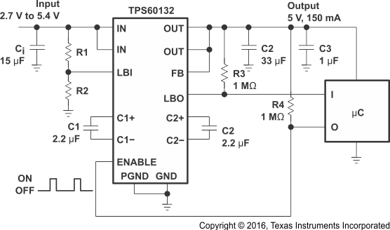 Figure 31. TPS60132 in Ultra-Low Quiescent Current Mode
10.2.2.1 Design Requirements
The device operates over an input voltage range from 2.7 V to 5.4 V.
10.2.3 Regulated Discharge of the Output Capacitors After Disabling of the TPS6013x
During shutdown of the charge pump TPS6013x the output is isolated from the input. Therefore, the discharging of the output capacitor depends on the load and on the leakage current of the capacitor. In certain applications it is necessary to completely remove the supply voltage from the load in shutdown mode. That means the output capacitor of the charge pump has to be actively discharged when the charge pump is disabled. Figure 5 shows one solution to this problem.
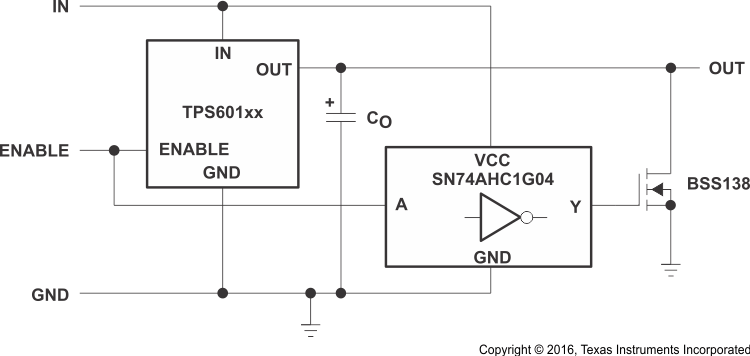 Figure 32. Block Diagram of the Regulated Discharge of the Output Capacitor
10.2.3.1 Design Requirements
The device operates over an input voltage range from 2.7 V to 5.4 V. TI's SN74AHC1G04 and BSS138 is required.