SLVSA02B September   2009  – January 2019 TPS60151

PRODUCTION DATA.  

  1. Features
  2. Applications
  3. Description
    1.     Device Images
      1.      Typical Application Schematic
      2.      Efficiency vs Input Voltage
  4. Revision History
  5. Device Comparison Table
  6. Pin Configuration and Functions
    1.     Pin Functions
  7. Specifications
    1. 7.1 Absolute Maximum Ratings
    2. 7.2 ESD Ratings
    3. 7.3 Recommended Operating Conditions
    4. 7.4 Thermal Information
    5. 7.5 Electrical Characteristics
    6. 7.6 Typical Characteristics
  8. Detailed Description
    1. 8.1 Overview
    2. 8.2 Functional Block Diagram
    3. 8.3 Feature Description
      1. 8.3.1 Enable
      2. 8.3.2 Output Reverse Current Protection
      3. 8.3.3 Undervoltage Lockout
      4. 8.3.4 Thermal Shutdown Protection
    4. 8.4 Device Functional Modes
      1. 8.4.1 Soft Start
      2. 8.4.2 Normal Mode and Skip Mode Operation
      3. 8.4.3 Over-current Protection and Short-Circuit Protection
  9. Application and Implementation
    1. 9.1 Application Information
    2. 9.2 Typical Application
      1. 9.2.1 Design Requirements
      2. 9.2.2 Detailed Design Procedure
        1. 9.2.2.1 Capacitor Selection
      3. 9.2.3 Application Curves
    3. 9.3 System Example
      1. 9.3.1 Circuit for Driving White LEDs
  10. 10Power Supply Recommendations
  11. 11Layout
    1. 11.1 Layout Guidelines
    2. 11.2 Layout Example
  12. 12Device and Documentation Support
    1. 12.1 Receiving Notification of Documentation Updates
    2. 12.2 Community Resources
    3. 12.3 Trademarks
    4. 12.4 Electrostatic Discharge Caution
    5. 12.5 Glossary
  13. 13Mechanical, Packaging, and Orderable Information

Package Options

Mechanical Data (Package|Pins)
Thermal pad, mechanical data (Package|Pins)
Orderable Information

Output Reverse Current Protection

Applications like HDMI or USB OTG generally do not tolerate output reverse current that can drain power from connected devices. Special considerations were put in place to prevent that from happening. Figure 5 is a testing circuit; and, Figure 6 shows reverse current protection test results under various conditions.

TPS60151 tst_setup_lvsa02.gifFigure 5. Output Reverse Current Test Setup
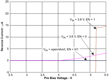
TPS60151 rev_curr_lvsa02.gifFigure 6. Reverse Current Test Results (Typical)