SLVS274A March 2000 – April 2016 TPS60200 , TPS60201 , TPS60202 , TPS60203
PRODUCTION DATA.
- 1 Features
- 2 Applications
- 3 Description
- 4 Revision History
- 5 Device Comparison Tables
- 6 Pin Configuration and Functions
- 7 Specifications
- 8 Detailed Description
- 9 Application and Implementation
- 10Power Supply Recommendations
- 11Layout
- 12Device and Documentation Support
- 13Mechanical, Packaging, and Orderable Information
Package Options
Mechanical Data (Package|Pins)
- DGS|10
Thermal pad, mechanical data (Package|Pins)
Orderable Information
9 Application and Implementation
NOTE
Information in the following applications sections is not part of the TI component specification, and TI does not warrant its accuracy or completeness. TI’s customers are responsible for determining suitability of components for their purposes. Customers should validate and test their design implementation to confirm system functionality.
9.1 Application Information
The power-good output is an open-drain output that pulls low when the output is out of regulation. When the output rises to within 90% of its nominal voltage, the power-good output is released. Power-good is high impedance in shutdown. In normal operation, an external pullup resistor must be connected between PG and OUT, or any other voltage rail in the appropriate range. The resistor should be in the 100-k Ω to 1-M Ω range. If the PG output is not used, it should remain unconnected)
9.1.1 Capacitor Selection
The TPS6020x devices require only four external capacitors to achieve a very low output voltage ripple. The capacitor values are closely linked to the required output current. Low ESR (<0.1 Ω) capacitors should be used at input and output. In general, the transfer capacitors (C1 and C2) will be the smallest, a 1-µF value is recommended for maximum load operation. With smaller capacitor values, the maximum possible load current is reduced and the LinSkip threshold is lowered.
The input capacitor improves system efficiency by reducing the input impedance. It also stabilizes the input current of the power source. The input capacitor should be chosen according to the power supply used and the distance from the power source to the converter IC. TI recommends Ci be about two to four times as large as the flying capacitors C1 and C2.
The output capacitor (Co) should be at minimum the size of the input capacitor. The minimum required capacitance is 2.2 μF. Larger values will improve the load transient performance and will reduce the maximum output ripple voltage.
Only ceramic capacitors are recommended for input, output, and flying capacitors. Depending on the material used to manufacture them, ceramic capacitors might lose their capacitance over temperature and voltage. Ceramic capacitors of type X7R or X5R material will keep their capacitance over temperature and voltage, whereas Z5U- or Y5V-type capacitors will decrease in capacitance. Table 3 lists the recommended capacitor values.
Table 3. Recommended Capacitors Values (Ceramic X5R and X7R)
| LOAD CURRENT, IL (mA) | FLYING CAPACITORS, C1/C2 (µF) | INPU CAPACITOR, Ci (µF) | OUTPUT CAPACITOR, Co (µF) | OUTPUT VOLTAGE RIPPLE IN LINEAR MODE, V(P-P) (mV) | OUTPUT VOLTAGE RIPPLE IN SKIP MODE, V(P-P) (mV) |
|---|---|---|---|---|---|
| 0 to 100 | 1 | 2.2 | 2.2 | 3 | 20 |
| 0 to 100 | 1 | 4.7 | 4.7 | 3 | 10 |
| 0 to 100 | 1 | 2.2 | 10 | 3 | 7 |
| 0 to 100 | 2.2 | 4.7 | 4.7 | 3 | 10 |
| 0 to 50 | 0.47 | 2.2 | 2.2 | 3 | 20 |
| 0 to 25 | 0.22 | 2.2 | 2.2 | 5 | 15 |
| 0 to 10 | 0.1 | 2.2 | 2.2 | 5 | 15 |
9.2 Typical Applications
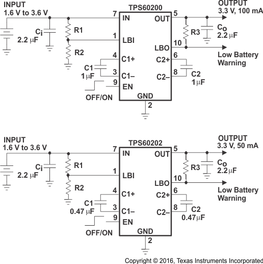 Figure 4. Typical Operating Circuit TPS60200 and TPS60202 With Low-Battery-Detector
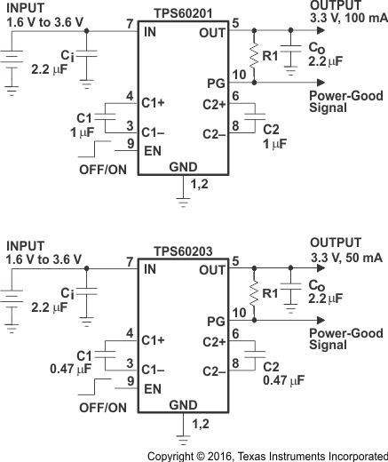 Figure 5. Typical Operating Circuit TPS60201 and TPS60203 With Power-Good-Detector
9.2.1 Design Requirements
Table 4 lists the capacitor selections to operate the device in the recommended operating conditions.
Table 4. Recommended Capacitor Types
| MANUFACTURER | PART NUMBER | SIZE | CAPACITANCE | TYPE |
|---|---|---|---|---|
| Taiyo Yuden | UMK212BJ104MG | 0805 | 0.1 µF | Ceramic |
| Taiyo Yuden | EMK212BJ224MG | 0805 | 0.22 µF | Ceramic |
| Taiyo Yuden | EMK212BJ474MG | 0805 | 0.47 µF | Ceramic |
| Taiyo Yuden | LMK212BJ105KG | 0805 | 1 µF | Ceramic |
| Taiyo Yuden | LMK212BJ225MG | 0805 | 2.2 µF | Ceramic |
| Taiyo Yuden | EMK316BJ225KL | 1206 | 2.2 µF | Ceramic |
| Taiyo Yuden | LMK316BJ475KL | 1206 | 4.7 µF | Ceramic |
| Taiyo Yuden | JMK316BJ106ML | 1206 | 10 µF | Ceramic |
| AVX | 0805ZC105KAT2A | 0805 | 1 µF | Ceramic |
| AVX | 1206ZC225KAT2A | 1206 | 2.2 µF | Ceramic |
9.2.2 Detailed Design Procedure
9.2.2.1 Low-Battery Detector (TPS60200 and TPS60202)
The low-battery comparator trips at 1.18 V ±4% when the voltage on pin LBI ramps down. The voltage V (TRIP) at which the low-battery warning is issued can be adjusted with a resistive divider as shown in Figure 4. The sum of resistors R1 and R2 is recommended to be in the 100-kΩ to 1-MΩ range. When choosing R1 and R2, be aware of the input leakage current into the LBI pin.
LBO is an open-drain output. TI recommends an external pullup resistor to OUT, or any other voltage rail in the appropriate range, in the 100-kΩ to 1-MΩ range. During start-up, the LBO output signal is invalid for the first 500 μs. LBO is high impedance when the device is disabled. If the low-battery comparator function is not used, connect LBI to ground and leave LBO unconnected. The low-battery detector is disabled when the device is switched off.
space
 Figure 6. Programming of the Low-Battery Comparator Trip Voltage
space
A 100-nF ceramic capacitor should be connected in parallel to R2 if large line transients are expected. These voltage drops can inadvertently trigger the low-battery comparator and produce a wrong low-battery warning signal at the LBO pin.
Formulas to calculate the resistive divider for low-battery detection, with V LBI = 1.13 V to 1.23 V and the sum of resistors R1 and R2 equal 1 MΩ.
space


space
Formulas to calculate the minimum and maximum battery voltage.
space


space
Table 5. Recommended Values for the Resistive Divider From the E96 Series (±1%)
| V(IN)/V | R1/kΩ | R2/kΩ | VTRIP(MIN)/V | VTRIP(MAX)/V |
|---|---|---|---|---|
| 1.6 | 267 | 750 | 1.524 | 1.677 |
| 1.7 | 301 | 681 | 1.62 | 1.785 |
| 1.8 | 340 | 649 | 1.71 | 1.887 |
| 1.9 | 374 | 619 | 1.799 | 1.988 |
| 2 | 402 | 576 | 1.903 | 2.106 |
9.2.3 Application Curves
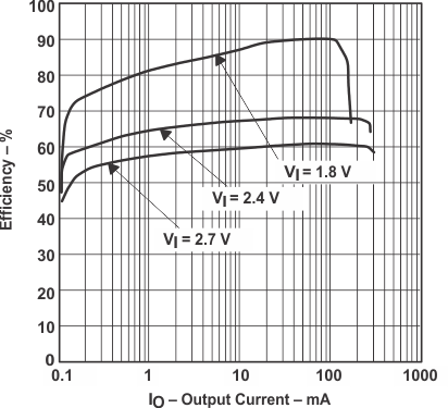 Figure 7. TPS60200 Efficiency vs Output Current
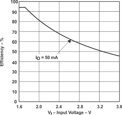 Figure 9. TPS60200 Efficiency vs Input Voltage
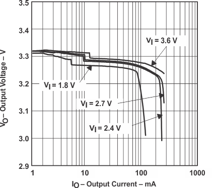 Figure 11. TPS60200 Output Voltage vs Output Current
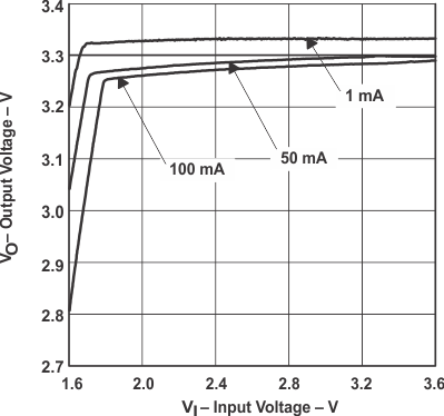 Figure 13. TPS60200 Output Voltage vs Input Voltage
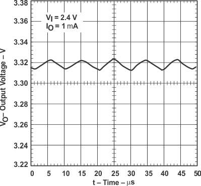 Figure 15. TPS60200 Output Voltage Ripple
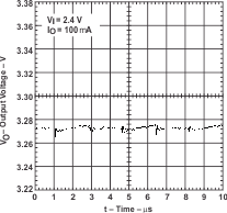 Figure 17. TPS60200 Output Voltage Ripple
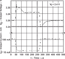 Figure 19. TPS60200 Load Transient Response
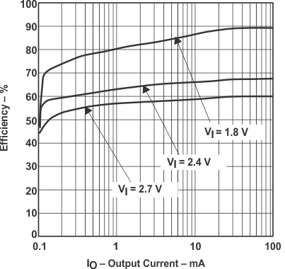 Figure 8. TPS60202 Efficiency vs Output Current
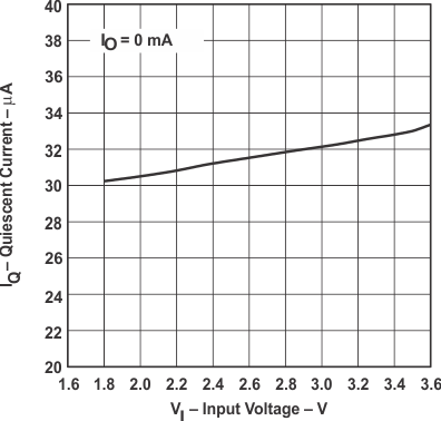 Figure 10. Quiescent Supply Current vs Input Voltage
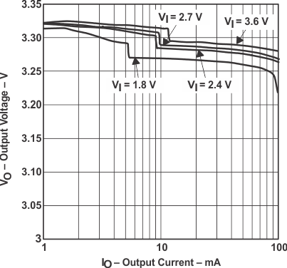 Figure 12. TPS60202 Output Voltage vs Output Current
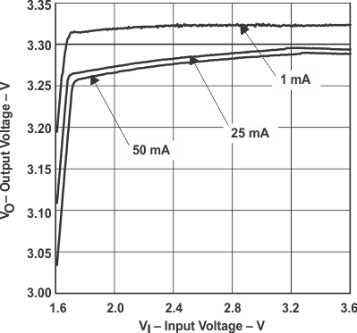 Figure 14. TPS60202 Output Voltage vs Input Voltage
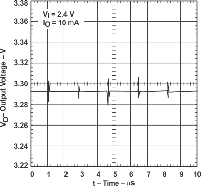 Figure 16. TPS60200 Output Voltage Ripple
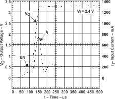 Figure 18. Start-Up Timing
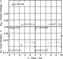 Figure 20. TPS60200 Line Transient Response