SLVS354B february 2001 – may 2023 TPS60204
PRODUCTION DATA
- 1
- 1 Features
- 2 Applications
- 3 Description
- 4 Revision History
- 5 Description (continued)
- 6 Pin Configuration and Functions
- 7 Specifications
- 8 Detailed Description
- 9 Application and Implementation
- 10Device and Documentation Support
- 11Mechanical, Packaging, and Orderable Information
Package Options
Mechanical Data (Package|Pins)
- DGS|10
Thermal pad, mechanical data (Package|Pins)
Orderable Information
7.7 Typical Characteristics
Table 7-1 Table of Graphs
| FIGURES | |||
|---|---|---|---|
| η | Efficiency | vs Output current (TPS60204, TPS60205) | 7-1 |
| vs Input voltage | 7-2 | ||
| IQ | Quiescent supply current | vs Input voltage | 7-3 |
| VO | Output voltage | vs Output current | 7-4 |
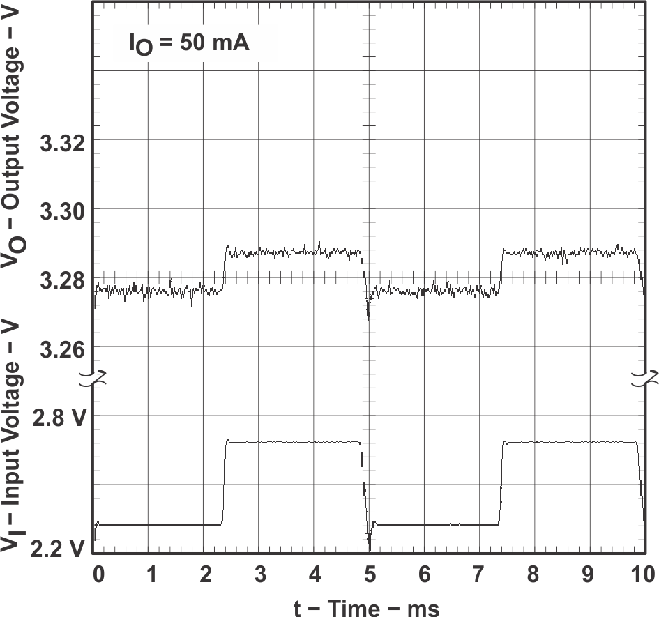
| vs Input voltage | 7-5 | ||
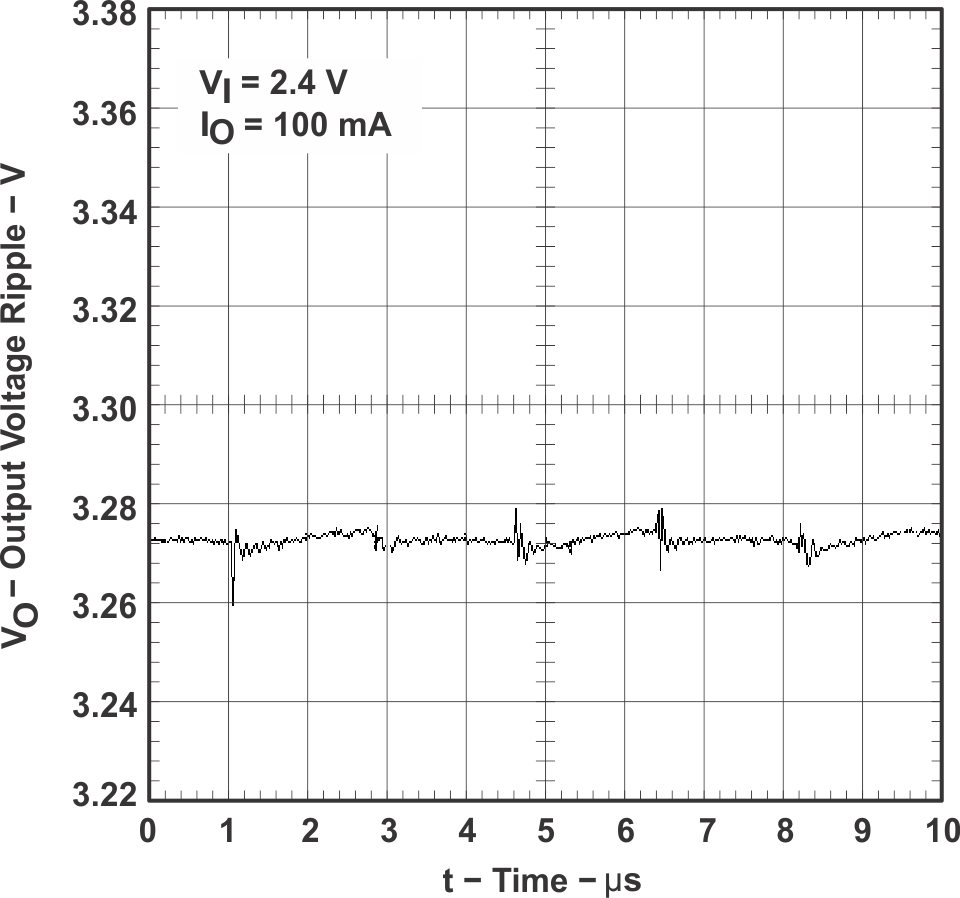
| VO | Output voltage ripple | vs Time | 7-6, 7-7, 7-8 |
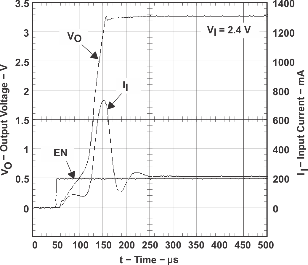
| Start-up timing | 7-9 | ||
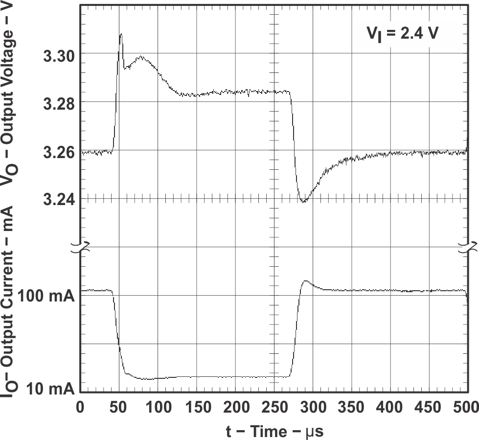
| Load transient response | 7-10, 7-11 | ||
| IO | Peak output current | vs Input voltage | 7-12 |
 Figure 7-1 TPS60204, TPS60205 Efficiency vs Output Current
 Figure 7-3 Quiescent Supply Current
vs Input Voltage
 Figure 7-5 Output Voltage vs Input
Voltage
 Figure 7-7 Output Voltage Ripple vs
Time
 Figure 7-9 Start-Up Timing
 Figure 7-11 Line Transient
Response
 Figure 7-2 Efficiency vs Input
Voltage
 Figure 7-4 Output Voltage vs Output
Current
 Figure 7-6 Output Voltage Ripple vs
Time
 Figure 7-8 Output Voltage Ripple vs
Time
 Figure 7-10 Load Transient
Response
 Figure 7-12 Peak Output Current vs
Input Voltage