SLVS302B December 2000 – October 2015 TPS60300 , TPS60301 , TPS60302 , TPS60303
PRODUCTION DATA.
- 1 Features
- 2 Applications
- 3 Description
- 4 Revision History
- 5 Description (continued)
- 6 Device Comparison Table
- 7 Pin Configuration and Functions
- 8 Specifications
- 9 Detailed Description
- 10Application and Implementation
- 11Power Supply Recommendations
- 12Layout
- 13Device and Documentation Support
- 14Mechanical, Packaging, and Orderable Information
Package Options
Mechanical Data (Package|Pins)
- DGS|10
Thermal pad, mechanical data (Package|Pins)
Orderable Information
10 Application and Implementation
NOTE
Information in the following applications sections is not part of the TI component specification, and TI does not warrant its accuracy or completeness. TI’s customers are responsible for determining suitability of components for their purposes. Customers should validate and test their design implementation to confirm system functionality.
10.1 Application Information
The TPS6030x is a switched capacitor voltage converter providing low noise, constant-frequency linear regulation mode. It supports regulated output voltages of 3 V and 3.3 V from a 0.9-V to 1.8-V input voltage range.
10.2 Typical Application
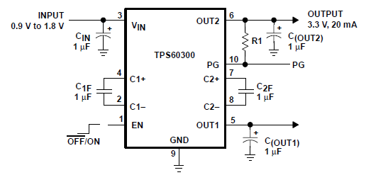 Figure 3. Typical Operating Circuit
10.2.1 Design Requirements
The complete charge pump circuitry requires no inductors and only five small 1-µF ceramic capacitors. It is possible to only use 1-µF capacitors of the same type.
10.2.2 Detailed Design Procedure
10.2.2.1 Capacitor Selection
The values of the five external capacitors of the TPS6030x charge pumps are closely linked to the required output current and the output noise and ripple requirements.
For the maximum output current and best performance, five ceramic capacitors with a minimum value of 1 µF are recommended. This value is necessary to assure a stable operation of the system due to the linear mode. For lower currents or higher allowed output voltage ripple, other capacitors can be used. With flying capacitors lower than 1 µF, the maximum output power will decrease. This means that the device will work in the linear mode with lower output currents.
The input capacitor improves system efficiency by reducing the input impedance and stabilizing the input current.
The minimum required capacitance of the output capacitor (COUT) that can be selected is 1 µF. Depending on the maximum allowed output ripple voltage, larger values can be chosen. Table 1 shows capacitor values recommended for low output voltage ripple operation. A recommendation is given for the smallest size.
Table 1. Recommended Capacitor Values for Low Output Voltage Ripple Operation
| VIN
[V] |
IOUT(OUT2)
[mA] |
CIN
[µF] |
CXF
[µF] |
COUT
[µF] |
VP-P [mV] At 20 mA / VIN = 1.1 V |
|---|---|---|---|---|---|
| CERAMIC | CERAMIC | CERAMIC | |||
| 0.9...1.8 | 0...20 | 1 | 1 | 1 | 16 |
| 0.9...1.8 | 0...20 | 1 | 1 | 2.2 | 10 |
| 0.9...1.8 | 0…20 | 1 | 1 | 10 // 0.1 | 6 |
Table 2. Recommended Capacitors
| MANUFACTURER | PART NUMBER | SIZE | CAPACITANCE | TYPE |
|---|---|---|---|---|
| Taiyo Yuden | UMK212BJ104MG LMK212BJ105KG LMK212BJ225MG JMK316BJ475KL |
805 805 805 1206 |
0.1 µF 1 µF 2.2 µF 4.7 µF |
Ceramic Ceramic Ceramic Ceramic |
| AVX | 0805ZC105KAT2A 1206ZC225KAT2A |
805 1206 |
1 µF 2.2 µF |
Ceramic Ceramic |
Table 3 lists the manufacturers of recommended capacitors. However, ceramic capacitors will provide the lowest output voltage ripple due to their typically lower ESR.
Table 3. Recommended Capacitor Manufacturers
| MANUFACTURER | CAPACITOR TYPE | INTERNET |
|---|---|---|
| Taiyo Yuden | X7R/X5R ceramic | www.t-yuden.com |
| AVX | X7R/X5R ceramic | www.avxcorp.com |
| Vishay | X7R/X5R ceramic | www.vishay.com |
| Kemet | X7R/X5R ceramic | www.kemet.com |
| TDK | X7R/X5R ceramic | www.component.tdk.com |
10.2.2.2 Output Filter Design
The power-good output is capable of driving light loads up to 5 mA (see Figure 4). Therefore, the output resistance of the power-good pin, in addition with an output capacitor, can be used as an RC-filter.
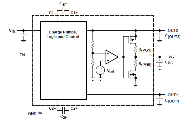 Figure 4. TPS60302, TPS60303 Push-Pull Power-Good Output-Stage as Filtered Supply
Due to R(PG,1), an output filter can easily be formed with an output capacitor (CPG). Cut-off frequency is given by:


with R(PG,1) = 15 Ω, C(PG) = 0.1 µF and f = 600 kHz (at nominal switching frequency)

Load current sourced by power-good output reduces maximum output current at OUT2. During start-up (power good going high) current charging C(PG) will discharge C(OUT2). Therefore, C(PG) must not be larger than 0.1 C(OUT2) or the device will not start. By charging C(PG) through C(OUT2), the output voltage at OUT2 will decrease. If the capacitance of C(PG) is to large, the circuit will detect power bad. The power-good output will go low and discharge C(PG). Then the cycle starts again. Figure 5 shows a configuration with an LC-post filter to further reduce output ripple and noise.
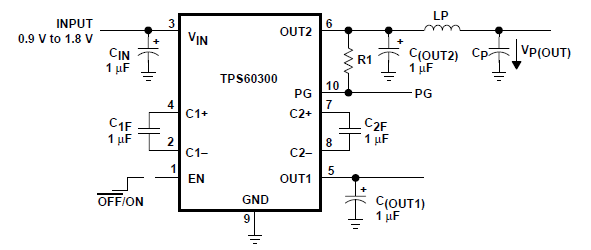 Figure 5. LC-Post Filter
Table 4. Recommended Values for Lowest Output Voltage Ripple
| VIN
[V] |
IO(OUT2)
[mA] |
CIN[µF] | CXF[µF] | COUT[µF] | LP[µH] | CP[µF] | VP(OUT)
VP-P[mV] |
|---|---|---|---|---|---|---|---|
| CERAMIC | CERAMIC | CERAMIC | CERAMIC | ||||
| 0.9...1.8 | 20 | 1 | 1 | 1 | 0.1 | 0.1 (X7R) | 16 |
| 0.9...1.8 | 20 | 1 | 1 | 1 | 0.1 | 1 // 0.1 (X7R) | 12 |
| 0.9...1.8 | 20 | 1 | 1 | 1 | 1 | 0.1 (X7R) | 14 |
| 0.9...1.8 | 20 | 1 | 1 | 10 | 1 | 1 // 0.1 (X7R) | 3 |
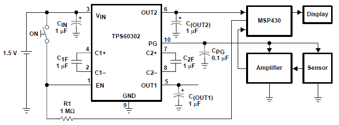 Figure 6. Application With MSP430; PG as Supply for Analog Circuits
10.2.3 Application Curves
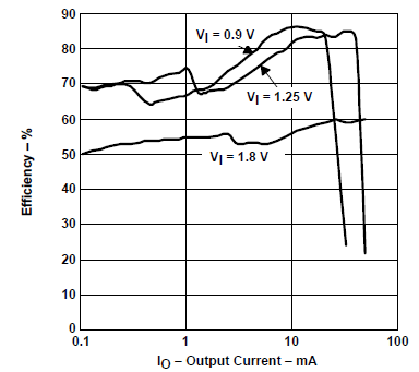 Figure 7. TPS60300, TPS60302
 Efficiency vs Output Current
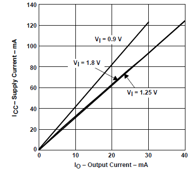 Figure 9. TPS60300
Supply Current vs Output Current
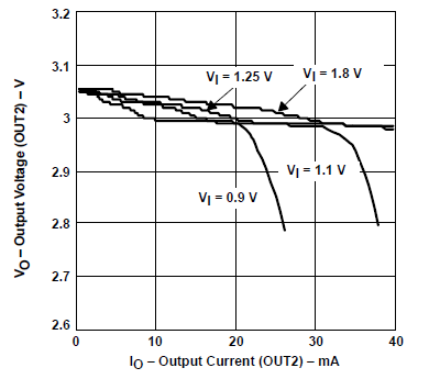 Figure 11. TPS60301, TPS60303
 Output Voltage (OUT2) vs Output Current (OUT2)
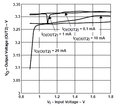 Figure 13. TPS60300, TPS60302
 Output Voltage (OUT2) vs Input Voltage
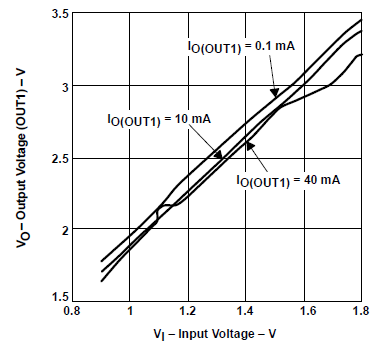 Figure 15. TPS6030x
 Output Voltage (OUT1) vs Input Voltage
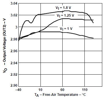 Figure 17. TPS60301, TPS60303
 Output Voltage (OUT2) vs Free-Air Temperature
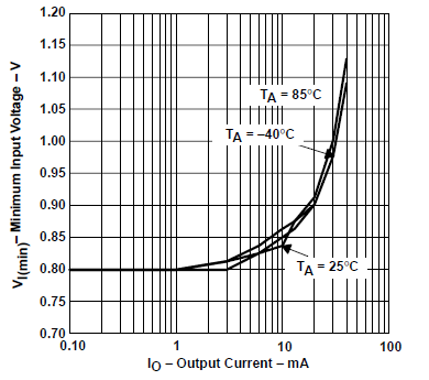 Figure 19. TPS60300, TPS60302
 Minimum Input Voltage vs Output Current
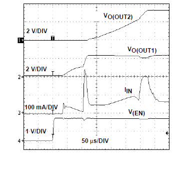 Figure 21. Start-Up Timing Enable
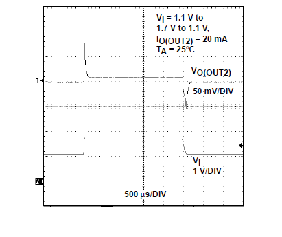 Figure 23. Line Transient Response
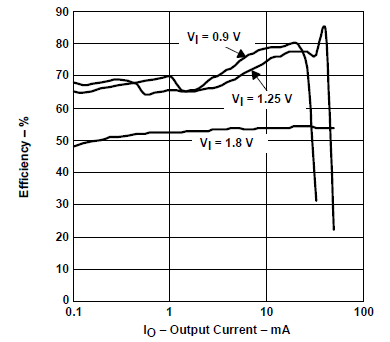 Figure 8. TPS60301, TPS60303
 Efficiency vs Output Current
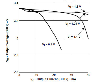 Figure 10. TPS60300, TPS60302
 Output Voltage (OUT2) vs Output Current (OUT2)
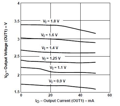 Figure 12. TPS60300, TPS60302
 Output Voltage (OUT1) vs Output Current (OUT1)
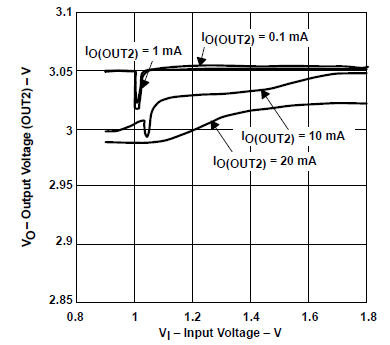 Figure 14. TPS60300, TPS60302
 Output Voltage (OUT2) vs Input Voltage
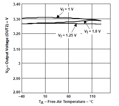 Figure 16. TPS60300, TPS60302
 Output Voltage (OUT2) vs Free-Air Temperature
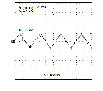 Figure 18. TPS6030x
 Output Voltage Ripple (OUT2)
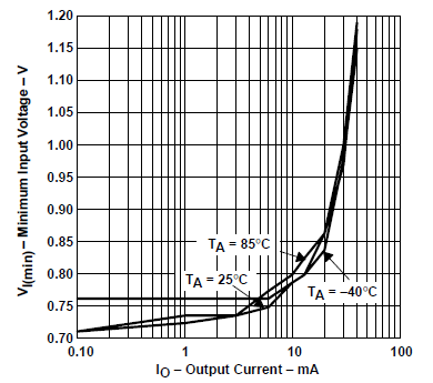 Figure 20. TPS60301, TPS60303
 Minimum Input Voltage vs Output Current
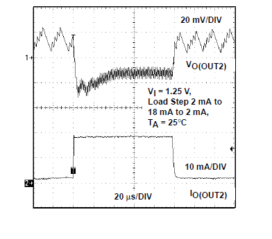 Figure 22. Load Transient Response