SLVS302B December 2000 – October 2015 TPS60300 , TPS60301 , TPS60302 , TPS60303
PRODUCTION DATA.
- 1 Features
- 2 Applications
- 3 Description
- 4 Revision History
- 5 Description (continued)
- 6 Device Comparison Table
- 7 Pin Configuration and Functions
- 8 Specifications
- 9 Detailed Description
- 10Application and Implementation
- 11Power Supply Recommendations
- 12Layout
- 13Device and Documentation Support
- 14Mechanical, Packaging, and Orderable Information
Package Options
Mechanical Data (Package|Pins)
- DGS|10
Thermal pad, mechanical data (Package|Pins)
Orderable Information
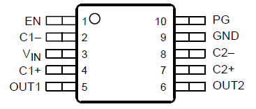
7 Pin Configuration and Functions
DGS Package
10-Pin VSSOP
Top View

Pin Functions
| PIN | I/O | DESCRIPTION | |
|---|---|---|---|
| NAME | NO. | ||
| C1+ | 4 | — | Positive pin of the flying capacitor C1F |
| C1– | 2 | — | Negative pin of the flying capacitor C1F |
| C2+ | 7 | — | Positive pin of the flying capacitor C2F |
| C2– | 8 | — | Negative pin of the flying capacitor C2F |
| EN | 1 | I | Device-enable input – EN = Low disables the device. Output and input are isolated in shutdown mode. – EN = High enables the device. |
| GND | 9 | — | Ground |
| OUT1 | 5 | O | 2 × VIN power output. Bypass OUT1 to GND with the output filter capacitor C(OUT1). |
| OUT2 | 6 | O | Regulated 3.3-V power output (TPS60300, TPS60302) or 3-V power output (TPS60301, TPS60303), respectively Bypass OUT2 to GND with the output filter capacitor C(OUT2). |
| PG | 10 | O | Power good detector output. As soon as the voltage on OUT2 reaches about 98% of its nominal value this pin goes high. Open-drain output on TPS60300 and TPS60301. A pull-up resistor should be connected between PG and OUT1 or OUT2. Push-pull output stage on TPS60302 and TPS60303 |
| VIN | 3 | I | Supply input. Bypass VIN to GND with a ≥1-µF capacitor. |