SLVS324C July 2001 – October 2020 TPS60400 , TPS60401 , TPS60402 , TPS60403
PRODUCTION DATA
- 1 Features
- 2 Applications
- 3 Description
- 4 Revision History
- 5 Device Comparison Table
- 6 Pin Configuration and Functions
- 7 Specifications
- 8 Detailed Description
- 9 Application and Implementation
- 10Power Supply Recommendations
- 11Layout
- 12Device and Documentation Support
- 13Mechanical, Packaging, and Orderable Information
Package Options
Refer to the PDF data sheet for device specific package drawings
Mechanical Data (Package|Pins)
- DBV|5
Thermal pad, mechanical data (Package|Pins)
Orderable Information
8.4.1 Active-Schottky Diode
For a short period of time, when the input voltage is applied, but the inverter is not yet working, the output capacitor is charged positive by the load. To prevent the output being pulled above GND, a Schottky diode must be added in parallel to the output. The function of this diode is integrated into the TPS6040x devices, which gives a defined startup performance and saves board space.
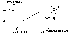
A current sink and a diode in series can approximate the behavior of a typical, modern operational amplifier. Figure 8-2 shows the current into this typical load at a given voltage. The TPS6040x devices are optimized to start into these loads.
 Figure 8-2 Typical Load
 Figure 8-3 Maximum Start-Up Current