SLVS324C July 2001 – October 2020 TPS60400 , TPS60401 , TPS60402 , TPS60403
PRODUCTION DATA
- 1 Features
- 2 Applications
- 3 Description
- 4 Revision History
- 5 Device Comparison Table
- 6 Pin Configuration and Functions
- 7 Specifications
- 8 Detailed Description
- 9 Application and Implementation
- 10Power Supply Recommendations
- 11Layout
- 12Device and Documentation Support
- 13Mechanical, Packaging, and Orderable Information
Package Options
Refer to the PDF data sheet for device specific package drawings
Mechanical Data (Package|Pins)
- DBV|5
Thermal pad, mechanical data (Package|Pins)
Orderable Information
8.1 Overview
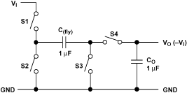
The TPS60400, TPS60401 charge pumps invert the voltage applied to their input. For the highest performance, use low equivalent series resistance (ESR) capacitors (for example, ceramic). During the first half-cycle, switches S2 and S4 open, switches S1 and S3 close, and capacitor (C(fly)) charges to the voltage at VI. During the second half-cycle, S1 and S3 open, S2 and S4 close. This connects the positive terminal of C(fly) to GND and the negative to VO. By connecting C(fly) in parallel, CO is charged negative. The actual voltage at the output is more positive than -VI, since switches S1-S4 have resistance and the load drains charge from CO.
 Figure 8-1 Operating Principle