SLVS391C October 2001 – September 2015 TPS60500 , TPS60501 , TPS60502 , TPS60503
PRODUCTION DATA.
- 1 Features
- 2 Applications
- 3 Description
- 4 Revision History
- 5 Device Comparison Table
- 6 Pin Configuration and Functions
- 7 Specifications
- 8 Detailed Description
- 9 Application and Implementation
- 10Power Supply Recommendations
- 11Layout
- 12Device and Documentation Support
- 13Mechanical, Packaging, and Orderable Information
Package Options
Mechanical Data (Package|Pins)
- DGS|10
Thermal pad, mechanical data (Package|Pins)
Orderable Information
8 Detailed Description
8.1 Overview
The TPS6050x charge pumps provide a regulated output voltage in the range of 0.8 V to 3.3 V from an input voltage of 1.8 V to 6.5 V. The devices use switched capacitor fractional conversion to achieve high efficiency over the entire input and output voltage range. Regulation is achieved by sensing the output voltage and enabling the internal switches as needed to maintain the selected output voltage. This skip-mode regulation is used over a load range from 0 mA to 150 mA. At a higher output current, the device works in a linear regulation mode.
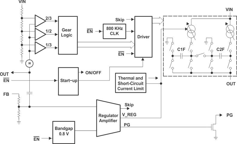
The TPS6050x circuits consist of an oscillator, a voltage reference, an internal resistive feedback circuit (fixed-voltage version only), an error amplifier, two charge pump stages with MOSFET switches, a shutdown or start-up circuit, and a control circuit.
8.2 Functional Block Diagram

8.3 Feature Description
8.3.1 Short-Circuit Current Limit and Thermal Protection
When the output voltage is lower than 0.6 V, the output current is limited to 300 mA typically.
The device also has a thermal protection which reduces the output current when the temperature of the chip exceeds 150°C. The output current declines to 0 mA when the chip temperature rises to 160°C.
8.3.2 Enable
Driving EN high disables the converter. This disables all internal circuits, reducing input current to only 0.05 µA. Leakage current drawn from the output pin OUT is a maximum of 1 µA. The device exits shutdown once EN is set low (see Start-up Procedure). The typical no-load start-up time is 80 µs. When the device is disabled, the load is isolated from the input, an important feature in battery-operated products because it extends the battery shelf life.
8.3.3 Power Good Detector
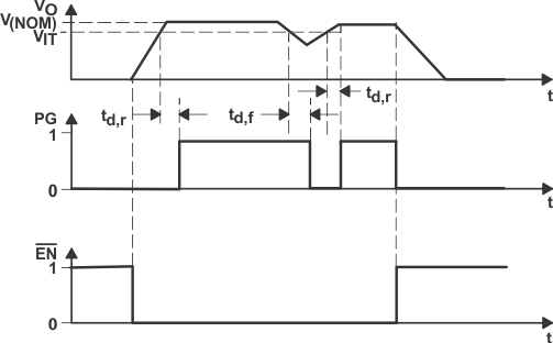
The power good (PG) output is an open-drain output on all TPS6050x devices. The PG output pulls low when the output is out of regulation. When the output rises above 97% nominal Vout, the power good output is pulled high by resistor. In shutdown, power good is pulled low. In normal operation, an external pullup resistor is typically used to connect the PG pin to VOUT or VIN. If the PG output is not used, it should remain unconnected.
 Figure 2. Power Good Timing Diagram
8.4 Device Functional Modes
8.4.1 Start-up Procedure
The device is enabled when EN is set from logic high to logic low. The charge pump stages immediately start switching to transfer energy to the output. In start-up until the output voltage has reached 0.6 V, the input current is limited to 300 mA typically.
8.4.2 Conversion Modes
The TPS6050x devices use fractional conversion to achieve high efficiency over a wide input and output voltage range. Depending on the input to output voltage ratio and output current, internal circuitry switches between an LDO mode, a 2/3x mode, a 0.5x mode, and a 1/3x mode.
8.4.2.1 LDO Conversion Mode
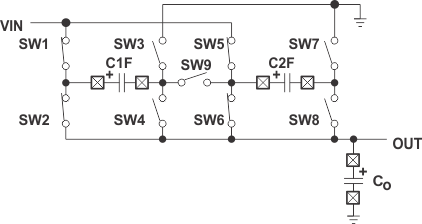
In the LDO mode, the flying capacitors are no longer used for transferring energy. The switches 1, 2, 5, and 6 are closed and connect the input directly with the output. This mode is automatically selected if the input to output voltage ratio does not allow the use of another conversion mode with higher efficiency. In LDO mode, the regulation is done by switching off MOSFET 2 and 6 until the output current reaches the linear-skip current (150 mA typical). At a higher output current, the output voltage is regulated by controlling the resistance of the switch. The minimum input to output voltage difference required for regulation is 1 V.
 Figure 3. LDO Conversion Mode
8.4.2.2 2/3x Conversion Mode
In the first cycle, the two flying capacitors are connected in parallel and are charged up in series with the output capacitor. In the second cycle, the flying capacitors are connected in series. This mode provides higher efficiency than the LDO mode because the current into VIN is only 2/3 of the output current. The mode is automatically selected if the input voltage is higher than 3/2 of the selected output voltage.
 Figure 4. 2/3x Conversion Mode
8.4.2.3 0.5x Conversion Mode
This conversion mode is internally selected if the input to output voltage ratio is greater than two (for example, 3.6-V to 1.5-V conversion). In the 0.5x mode, the flying capacitors and the switches always work in parallel, which reduces the resistance of the circuit compared to the other modes. In the first cycle, the flying capacitors are charged in series with the output capacitors. In the second cycle, the flying capacitors are connected in parallel with the output capacitor, which discharges the flying capacitors.
 Figure 5. 0.5x Conversion Mode
8.4.2.4 1/3x Conversion Mode
This mode was implemented to provide high efficiency even with an input to output voltage ratio greater than three (for example, 5-V to 1.5-V conversion). In the first cycle, the two flying capacitors are charged in series with the output capacitor. In the next step, the flying capacitors which are charged to VIN/3, are connected in parallel to the output capacitor.
 Figure 6. 1/3x Conversion Mode