-
TPS6100x Single- and Dual-Cell Boost Converter With Start-up Into Full Load
- 1 Features
- 2 Applications
- 3 Description
- 4 Revision History
- 5 Available Options
- 6 Pin Configuration and Functions
- 7 Specifications
- 8 Parameter Measurement Information
- 9 Detailed Description
- 10Application and Implementation
- 11Power Supply Recommendations
- 12Layout
- 13Device and Documentation Support
- 14Mechanical, Packaging, and Orderable Information
- IMPORTANT NOTICE
Refer to the PDF data sheet for device specific package drawings
Mechanical Data (Package|Pins)
- DGS|10
Thermal pad, mechanical data (Package|Pins)
TPS6100x Single- and Dual-Cell Boost Converter With Start-up Into Full Load
1 Features
- Start-Up Into a Full Load With Supply Voltages as Low as 0.9 V Over Full Temperature Range
- Minimum 100-mA Output Current From 0.8-V Supply Voltage, 250 mA From 1.8 V
- High Power Conversion Efficiency, up to 90%
- Power-Save Mode for Improved Efficiency at Low Output Currents
- Device Quiescent Current Less Than 50 µA
- Added System Security With Integrated Low-Battery Comparator
- Low-EMI Converter (Integrated Antiringing Switch Across Inductor)
- Micro-Size 10-Pin MSOP Package
- Evaluation Modules Available (TPS6100xEVM–156)
2 Applications
- Single- and Dual-Cell Battery Operated Products
- MP3-Players and Wireless Headsets
- Pagers and Cordless Phones
- Portable Medical Diagnostic Equipment
- Remote Controls
3 Description
The TPS6100x devices are boost converters intended for systems that are typically operated from a single- or dual-cell nickel-cadmium (NiCd), nickel-metal hydride (NiMH), or alkaline battery. The converter output voltage can be adjusted from 1.5 V to a maximum of 3.3 V and provides a minimum output current of 100 mA from a single battery cell and 250 mA from two battery cells. The converter starts up into a full load with a supply voltage of 0.9 V and stays in operation with supply voltages as low as 0.8 V.
The converter is based on a fixed-frequency, current-mode pulse-width-modulation (PWM) controller that goes into power-save mode at low load currents. The current through the switch is limited to a maximum of 1100 mA, depending on the output voltage. The current sense is integrated to further minimize external component count. The converter can be disabled to minimize battery drain when the system is put into standby.
A low-EMI mode is implemented to reduce interference and radiated electromagnetic energy that is caused by the ringing of the inductor when the inductor discharge-current decreases to zero. The device is packaged in the space-saving 10-pin MSOP package.
Device Information(1)
| PART NUMBER | PACKAGE | BODY SIZE (NOM) |
|---|---|---|
| TPS6100x | VSSOP (10) | 3.00 mm × 3.00 mm |
- For all available packages, see the orderable addendum at the end of the datasheet.
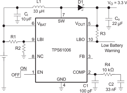
Typical Application Circuit for Fixed Output Voltage Options
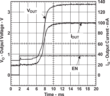
TPS61006 Start-Up Timing Into 33-Ω Load
4 Revision History
Changes from C Revision (April 2003) to D Revision
- Added Pin Configuration and Functions section, ESD Ratings table, Feature Description section, Device Functional Modes, Application and Implementation section, Power Supply Recommendations section, Layout section, Device and Documentation Support section, and Mechanical, Packaging, and Orderable Information section Go
- Replaced the Dissipation Ratings table with the Thermal Information tableGo
5 Available Options
| TA | PACKAGE | OUTPUT VOLTAGE (V) |
PART NUMBER(1) | MARKING DGS PACKAGE |
|---|---|---|---|---|
| –40°C to 85°C | 10-Pin MSOP DGS | Adj. from 1.5 V to 3.3 V | TPS61000DGS | ADA |
| 1.5 | TPS61001DGS | ADB | ||
| 1.8 | TPS61002DGS | ADC | ||
| 2.5 | TPS61003DGS | ADD | ||
| 2.8 | TPS61004DGS | ADE | ||
| 3.0 | TPS61005DGS | ADF | ||
| 3.3 | TPS61006DGS | ADG | ||
| Adj. from 1.5 V to 3.3 V | TPS61007DGS | AD |
6 Pin Configuration and Functions

Pin Functions
| PIN | I/O | DESCRIPTION | |
|---|---|---|---|
| NAME | NO. | ||
| COMP | 2 | — | Compensation of error amplifier. Connect R-C-C network to set frequency response of control loop. See the Application section for more details. |
| EN | 1 | I | Chip-enable input. The converter is switched on if EN is set high, and is switched off when EN is connected to ground (shutdown mode). |
| FB | 3 | I | Feedback input for adjustable output voltage (TPS61000 only). The output voltage is programmed depending on the values of resistors R1 and R2. For the fixed output voltage versions (TPS61000, TPS61002, TPS61003, TPS61004, TPS61005, TPS61006), leave the FB pin unconnected. |
| NC/FBGND | 8 | — | Not connected (TPS61000, TPS61002, TPS61003, TPS61004, TPS61005, TPS61006). A ground pin for the feedback resistor divider for the TPS61007 only. |
| GND | 4 | — | Ground |
| LBI | 9 | I | Low-battery detector input. A low-battery signal is generated at the LBO pin when the voltage on LBI drops below the threshold of 500 mV. Connect LBI to GND or VBAT if the low-battery detector function is not used. Do not leave this pin floating. |
| LBO | 10 | O | Open-drain low-battery detector output. This pin is pulled low if the voltage on LBI drops below the threshold of 500 mV. A pullup resistor should be connected between LBO and VOUT. |
| SW | 7 | I | Switch input pin. The node between inductor and anode of the rectifier diode is connected to this pin. |
| VBAT | 6 | I | Supply pin |
| VOUT | 5 | O | Output voltage. For the fixed output voltage versions, the integrated resistive divider is connected to this pin. |
7 Specifications
7.1 Absolute Maximum Ratings
over operating free-air temperature range (unless otherwise noted)(1)| MIN | MAX | UNIT | ||
|---|---|---|---|---|
| VI | Input voltage (VBAT, VOUT, COMP, FB, LBO, EN, LBI) | –0.3 | 3.6 | V |
| Input voltage (SW) | –0.3 | VOUT + 0.7 | V | |
| Peak current into SW | 1300 | mA | ||
| Continuous total power dissipation | See Thermal Information | |||
| TA | Operating free-air temperature | –40 | 85 | °C |
| TJ | Maximum junction temperature | 150 | °C | |
| Lead temperature | 260 | °C | ||
| Tstg | Storage temperature | –65 | 150 | °C |
7.2 ESD Ratings
| VALUE | UNIT | |||
|---|---|---|---|---|
| V(ESD) | Electrostatic discharge | Human body model (HBM), per ANSI/ESDA/JEDEC JS-001(1) | ±1000 | V |
| Charged-device model (CDM), per JEDEC specification JESD22-C101(2) | ±500 | |||
7.3 Recommended Operating Conditions
over operating free-air temperature range (unless otherwise noted)| MIN | NOM | MAX | UNIT | |||
|---|---|---|---|---|---|---|
| VBAT | Supply voltage | 0.8 | VO | V | ||
| VO | Output current | VBAT = 0.8 V | 100 | mA | ||
| VBAT = 0.8 V | 250 | |||||
| Inductor | 10 | 33 | µH | |||
| Input capacitor | 10 | µF | ||||
| Output capacitor | 22 | µF | ||||
| TJ | Operating junction temperature | –40 | 125 | °C | ||
7.4 Thermal Information
| THERMAL METRIC(1) | TPS6100x | UNIT | |
|---|---|---|---|
| DGS (VSSOP) | |||
| 10 PINS | |||
| RθJA | Junction-to-ambient thermal resistance | 160.6 | °C/W |
| RθJC(top) | Junction-to-case (top) thermal resistance | 54.4 | °C/W |
| RθJB | Junction-to-board thermal resistance | 80.5 | °C/W |
| ψJT | Junction-to-top characterization parameter | 6.3 | °C/W |
| ψJB | Junction-to-board characterization parameter | 79.2 | °C/W |
| RθJC(bot) | Junction-to-case (bottom) thermal resistance | N/A | °C/W |
7.5 Electrical Characteristics
over recommended operating free-air temperature range, VBAT = 1.2 V, EN = VBAT (unless otherwise noted)| PARAMETER | TEST CONDITIONS | MIN | TYP | MAX | UNIT | |||
|---|---|---|---|---|---|---|---|---|
| VI | Input voltage for start up | RL = 33 Ω | 0.9 | V | ||||
| RL = 3 kΩ, | TA = 25°C | 0.8 | ||||||
| Input voltage once started | IO = 100 mA | 0.8 | ||||||
| VO | Programmable output voltage | TPS61000, TPS61007 | IO = 100 mA | 1.5 | 3.3 | V | ||
| VO | Output voltage | TPS61001 | 1.2 V, | IO = 1 mA | 1.44 | 1.5 | 1.55 | V |
| 0.8 V < VI < VO, | IO = 100 mA | 1.45 | 1.5 | 1.55 | ||||
| TPS61002 | 1.2 V, | IO = 1 mA | 1,72 | 1.8 | 1.86 | V | ||
| 0.8 V < VI < VO, | IO = 100 mA | 1.74 | 1.8 | 1.86 | ||||
| TPS61003 | 1.2 V, | IO = 1 mA | 2.40 | 2.5 | 2.58 | V | ||
| 0.8 V < VI < VO, | IO = 100 mA | 2.42 | 2.5 | 2.58 | ||||
| 1.6 V < VI < VO, | IO = 200 mA | 2.42 | 2.5 | 2.58 | ||||
| TPS61004 | 1.2 V, | IO = 1 mA | 2.68 | 2.8 | 2.89 | V | ||
| 0.8 V < VI < VO, | IO = 100 mA | 2.72 | 2.8 | 2.89 | ||||
| 1.6 V < VI < VO, | IO = 200 mA | 2.72 | 2.8 | 2.89 | ||||
| TPS61005 | 1.2 V, | IO = 1 mA | 2.88 | 3.0 | 3.1 | V | ||
| 0.8 V < VI < VO, | IO = 100 mA | 2.9 | 3.0 | 3.1 | ||||
| 1.6 V < VI < VO, | IO = 200 mA | 2.9 | 3.0 | 3.1 | ||||
| TPS61006 | 1.2 V, | IO = 1 mA | 3.16 | 3.3 | 3.4 | V | ||
| 0.8 V < VI < VO, | IO = 100 mA | 3.2 | 3.3 | 3.4 | ||||
| 1.6 V < VI < VO, | IO = 200 mA | 3.2 | 3.3 | 3.4 | ||||
| IO | Maximum continuous output current | VI = 0.8 V | 100 | mA | ||||
| VI = 1.8 V | 250 | |||||||
| I ILIM | Switch current limit | TPS61001 | 0.8 V < VI < VO | 0.5 | A | |||
| TPS61002 | 0.65 | |||||||
| TPS61003 | 0.9 | |||||||
| TPS61004 | 0.95 | |||||||
| TPS61005 | 1 | |||||||
| TPS61006 | 1.1 | |||||||
| VFB | Feedback voltage | TPS61000, TPS61007 | 468 | 500 | 515 | mV | ||
| f | Oscillator frequency | 360 | 500 | 840 | kHz | |||
| DMAX | Maximum duty cycle | 85% | ||||||
| rDS(on) | Switch-on resistance | VO = 3.3 V | 0.18 | 0.27 | Ω | |||
| Line regulation (1) | VI = 0.8 V to 1.25 V, | IO = 50 mA | 0.3 | %/V | ||||
| Load regulation fixed output voltage versions (1) | VI = 1.2 V, | IO = 10 mA to 90 mA | 0.25% | |||||
| IQ | Quiescent current drawn from power source ower (current into VBAT and into VOUT) | IO = 0 mA, VEN = VI, VO = 3.4 V |
VBAT | 44 | µA | |||
| VOUT | 6 | |||||||
| ISD | Shutdown current from power source (current into VBAT and into VOUT) | VEN = 0 V | 0.2 | 5 | µA | |||
| VIL | EN low-level input voltage | 0.2x VBAT | V | |||||
| VIH | EN high-level input voltage | 0.8 × VBAT | V | |||||
| EN input current | EN = GND or VBAT | 0.1 | 1 | µA | ||||
| VIL | LBI low-level input voltage threshold | VLBI voltage decreasing | 470 | 500 | 530 | mV | ||
| LBI input hysteresis | 10 | |||||||
| II | LBI input current | 0.01 | 0.1 | µA | ||||
| VOL | LBO low-level output voltage | VLBI = 0 V, VO = 3.3 V, IOL = 50 µA | 0.04 | 0.2 | V | |||
| LBO output leakage current | VLBI = 650 mV, VLBO = 3.3 V | 0.01 | 1 | µA | ||||
| IFB | FB input bias current (TPS61000, TPS61007 only) | VFB = 500 mV | 0.01 | 0.1 | µA | |||
7.6 Typical Characteristics
Table 1. Table of Graphs
| TITLE | |||
|---|---|---|---|
| η | Efficiency | vs Output Current | Figure 1, Figure 2 |
| vs Inductor Type | Figure 3 | ||
| vs Input Voltage | Figure 4 | ||
| IO | Maximum Output Current | vs Input Voltage | Figure 5 |
| VO | Output Voltage | vs Output Current | Figure 6 |
| VO | TPS61007 Output Voltage | vs Output Current | Figure 7 |
| IQ | No-Load Supply Current | vs Input Voltage | Figure 8 |
| ISD | Shutdown Current | vs Input Voltage | Figure 9 |
| VI | Minimum Start-Up Input Voltage | vs Load Current | Figure 10 |
| ILIM | Switch Current Limit | vs Output Voltage | Figure 11 |
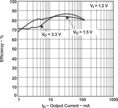 Figure 1. Efficiency vs Output Currency
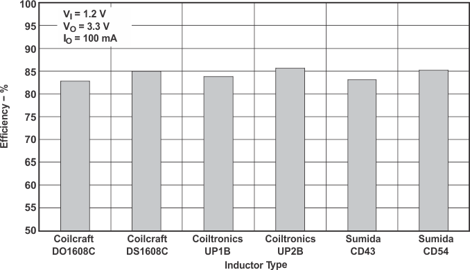 Figure 3. Efficiency vs Inductor Type
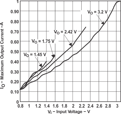 Figure 5. Maximum Output Current vs Input Voltage
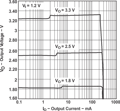 Figure 7. TPS61007 Output Voltage vs Output Current
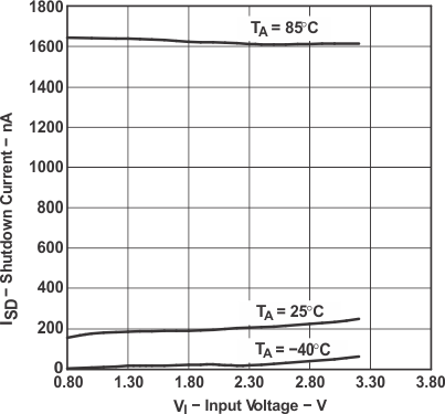 Figure 9. Shutdown Current vs Input Voltage
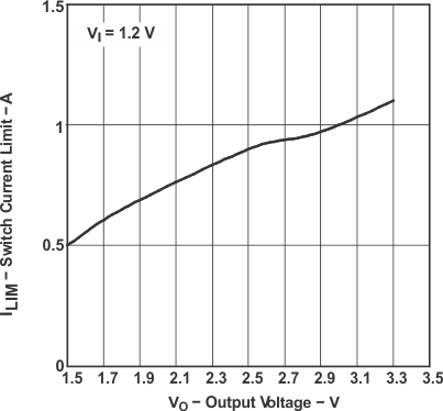 Figure 11. TPS61000, TPS61007 Switch Current Limit vs Output Voltage
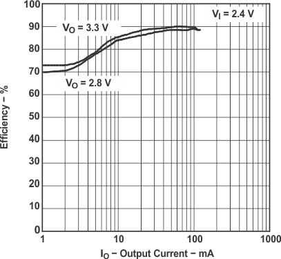 Figure 2. Efficiency vs Output Currency
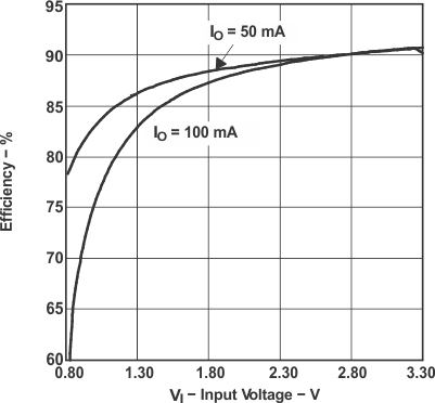 Figure 4. Efficiency vs Input Voltage
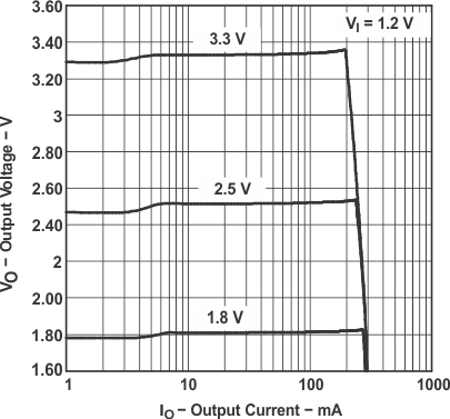 Figure 6. TPS61002/3/6 Output Voltage vs Output Current
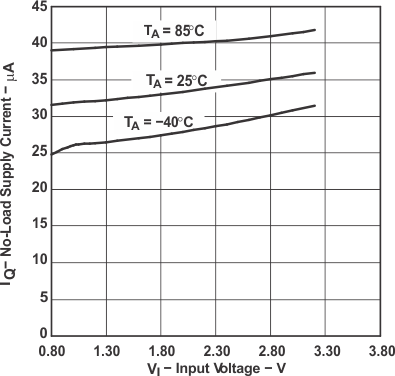 Figure 8. No-Load Supply Current vs Input Voltage
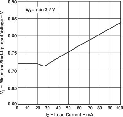 Figure 10. Minimum Start-up Input Voltage vs Load Current