SLVS279D March 2000 – August 2015 TPS61000 , TPS61002 , TPS61005 , TPS61006 , TPS61007
PRODUCTION DATA.
- 1 Features
- 2 Applications
- 3 Description
- 4 Revision History
- 5 Available Options
- 6 Pin Configuration and Functions
- 7 Specifications
- 8 Parameter Measurement Information
- 9 Detailed Description
- 10Application and Implementation
- 11Power Supply Recommendations
- 12Layout
- 13Device and Documentation Support
- 14Mechanical, Packaging, and Orderable Information
Refer to the PDF data sheet for device specific package drawings
Mechanical Data (Package|Pins)
- DGS|10
Thermal pad, mechanical data (Package|Pins)
9 Detailed Description
9.1 Overview
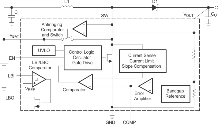
The TPS6100x Non-synchronous step-up converter typically operates at a 500-kHz frequency pulse width modulation (PWM) at moderate to heavy load currents. The converter enters Power Save mode at low load currents to maintain a high efficiency over a wide load. Additionally, the device integrates a circuit which removes the ringing that typically appears on the SW-node when the converter enters the discontinuous current mode.
9.2 Functional Block Diagrams
 Figure 13. Fixed Output-Voltage Option
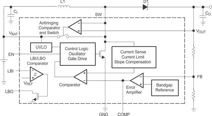
 Figure 14. Adjustable Output-Voltage Option (TPS61000 Only)
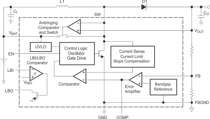
 Figure 15. Adjustable Output-Voltage Option (TPS61007 Only)
9.3 Feature Description
9.3.1 Controller Circuit
The device is based on a current-mode control topology using a constant-frequency pulse-width modulator to regulate the output voltage. It runs at an oscillator frequency of 500 kHz. The current sense is implemented by measuring the voltage across the switch. The controller also limits the current through the power switch on a pulse-by-pulse basis. Care must be taken that the inductor saturation current is higher than the current limit of the TPS6100x. This prevents the inductor from going into saturation and therefore protects both device and inductor. The current limit should not become active during normal operating conditions.
The TPS6100x is designed for high efficiency over a wide output current range. Even at light loads the efficiency stays high because the controller enters a power-save mode, minimizing switching losses of the converter. In this mode, the controller only switches if the output voltage trips below a set threshold voltage. It ramps up the output voltage with one or several pulses, and again goes into the power-save mode once the output voltage exceeds the threshold voltage. The controller enters the power-save mode when the output current drops to levels that force the discontinuous current mode. It calculates a minimum duty cycle based on input and output voltage and uses the calculation for the transition out of the power-save mode into continuous current mode.
The control loop must be externally compensated with an R/C/C network connected to the COMP pin. See the application section for more details on the design of the compensation network.
9.3.2 Device Enable
The device is put into operation when EN is set high. During start-up of the converter the input current from the battery is limited until the voltage on COMP reaches its operating point. The device is put into a shutdown mode when EN is set to GND. In this mode, the regulator stops switching and all internal control circuitry including the low-battery comparator is switched off. The output voltage drops to one diode drop below the input voltage in shutdown.
9.3.3 Undervoltage Lockout
An undervoltage lockout function prevents the device start-up if the supply voltage on VBAT is lower than approximately 0.7 V. This undervoltage lockout function is implemented in order to prevent the malfunctioning of the converter. When in operation and the battery is being discharged, the device automatically enters the shutdown mode if the voltage on VBAT drops below approximately 0.7 V.
If the EN pin is hardwired to VBAT and if the voltage at VBAT drops temporarily below the UVLO threshold voltage, the device switches off and does not start up again automatically, even if the supply voltage rises above 0.9 V. The device starts up again only after a signal change from low to high on EN or if the battery voltage is completely removed.
9.3.4 Low-Battery Detector Circuit (LBI and LBO)
The low-battery detector circuit is typically used to supervise the battery voltage and to generate an error flag when the battery voltage drops below a user-set threshold voltage. The function is active only when the device is enabled. When the device is disabled, the LBO pin is high impedance. The LBO pin goes active low when the voltage on the LBI pin decreases below the set threshold voltage of 500 mV ±15 mV, which is equal to the internal reference voltage. The battery voltage, at which the detection circuit switches, can be programmed with a resistive divider connected to the LBI pin. The resistive divider scales down the battery voltage to a voltage level of 500 mV, which is then compared to the LBI threshold voltage. The LBI pin has a built-in hysteresis of 10 mV. See the application section for more details about the programming of the LBI threshold.
If the low-battery detection circuit is not used, the LBI pin should be connected to GND (or to VBAT) and the LBO pin can be left unconnected. Do not let the LBI pin float.
9.3.5 Low-EMI Switch
The device integrates a circuit which removes the ringing that typically appears on the SW-node when the converter enters the discontinuous current mode. In this case, the current through the inductor ramps to zero and the Schottky diode stops conducting. Due to remaining energy that is stored in parasitic components of the diode, inductor, and switch, a ringing on the SW pin is induced. The integrated antiringing switch clamps this voltage internally to VBAT and therefore dampens this ringing.
The antiringing switch is turned on by a comparator that monitors the voltage between SW and VOUT. This voltage indicates when the diode is reverse biased. The ringing on the SW-node is damped to a large degree, reducing the electromagnetic interference generated by the switching regulator to a great extent.
9.3.6 Adjustable Output Voltage (TPS61000 and TPS61007 Only)
The accuracy of the internal voltage reference, the controller topology, and the accuracy of the external resistor divider determine the accuracy of the adjustable output voltage versions. The reference voltage has an accuracy of ±4% over line, load, and temperature. The controller switches between fixed frequency and pulse-skip mode, depending on load current. This adds an offset to the output voltage that is equivalent to 1% of VO. Using 1% accurate resistors for the feedback divider, a total accuracy of ±6% can be achieved over the complete temperature and output current range. The TPS61007 is an improved adjustable output voltage version. Ground shift in the feedback loop was eliminated by adding a separate ground pin for the feedback resistor divider (FBGND).
9.4 Device Functional Modes
9.4.1 Power Save Mode
The TPS6100x enters a power-save mode, minimizing switching losses of the converter. In this mode, the controller only switches if the output voltage trips below a set threshold voltage. It ramps up the output voltage with one or several pulses, and again goes into the power-save mode once the output voltage exceeds the threshold voltage.