SLVSA41B November   2009  – July 2016 TPS61085T

PRODUCTION DATA.  

  1. Features
  2. Applications
  3. Description
  4. Revision History
  5. Pin Configuration and Functions
  6. Specifications
    1. 6.1 Absolute Maximum Ratings
    2. 6.2 ESD Ratings
    3. 6.3 Recommended Operating Conditions
    4. 6.4 Thermal Information
    5. 6.5 Electrical Characteristics
    6. 6.6 Typical Characteristics
  7. Detailed Description
    1. 7.1 Overview
    2. 7.2 Functional Block Diagram
    3. 7.3 Feature Description
      1. 7.3.1 Soft Start
      2. 7.3.2 Frequency Select Pin (FREQ)
      3. 7.3.3 Undervoltage Lockout (UVLO)
      4. 7.3.4 Thermal Shutdown
      5. 7.3.5 Overvoltage Prevention
    4. 7.4 Device Functional Modes
  8. Application and Implementation
    1. 8.1 Application Information
    2. 8.2 Typical Application
      1. 8.2.1 Design Requirements
      2. 8.2.2 Detailed Design Procedure
        1. 8.2.2.1 Inductor Selection
        2. 8.2.2.2 Rectifier Diode Selection
        3. 8.2.2.3 Setting the Output Voltage
        4. 8.2.2.4 Compensation (COMP)
        5. 8.2.2.5 Input Capacitor Selection
        6. 8.2.2.6 Output Capacitor Selection
      3. 8.2.3 Application Curves
    3. 8.3 System Examples
  9. Power Supply Recommendations
  10. 10Layout
    1. 10.1 Layout Guidelines
    2. 10.2 Layout Example
  11. 11Device and Documentation Support
    1. 11.1 Device Support
      1. 11.1.1 Third-Party Products Disclaimer
    2. 11.2 Receiving Notification of Documentation Updates
    3. 11.3 Community Resources
    4. 11.4 Trademarks
    5. 11.5 Electrostatic Discharge Caution
    6. 11.6 Glossary
  12. 12Mechanical, Packaging, and Orderable Information

Package Options

Mechanical Data (Package|Pins)
Thermal pad, mechanical data (Package|Pins)
Orderable Information

1 Features

  • 2.3-V to 6-V Input Voltage Range
  • 18.5-V Boost Converter With 2-A Switch Current
  • 650-kHz or 1.2-MHz Selectable Switching Frequency
  • Adjustable Soft Start
  • Thermal Shutdown
  • Undervoltage Lockout
  • 8-Pin VSSOP and TSSOP Packages

2 Applications

  • Handheld Devices
  • GPS Receiver
  • Digital Still Camera
  • Portable Applications
  • DSL Modem
  • PCMCIA Card
  • TFT LCD Bias Supply

3 Description

The TPS61085 device is a high-frequency high-efficiency DC-to-DC boost converter with an integrated 2-A, 0.13-Ω power switch capable of providing an output voltage up to 18.5 V. The selectable frequency of 650 kHz or 1.2 MHz allows the use of small external inductors and capacitors, and provides fast transient response. The external compensation allows optimizing the regulator for application conditions. A capacitor connected to the specific soft-start pin minimizes inrush current at start-up.

Device Information(1)

PART NUMBER PACKAGE BODY SIZE (NOM)
TPS61085T VSSOP (8) 3.00 mm × 3.00 mm
TSSOP (8) 3.00 mm × 4.40 mm
  1. For all available packages, see the orderable addendum at the end of the data sheet.

Typical Application
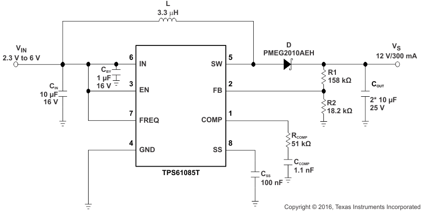
TPS61085T typ_app_cir_SLVSA41.gif