SLVSA41B November 2009 – July 2016 TPS61085T
PRODUCTION DATA.
- 1 Features
- 2 Applications
- 3 Description
- 4 Revision History
- 5 Pin Configuration and Functions
- 6 Specifications
- 7 Detailed Description
- 8 Application and Implementation
- 9 Power Supply Recommendations
- 10Layout
- 11Device and Documentation Support
- 12Mechanical, Packaging, and Orderable Information
Package Options
Mechanical Data (Package|Pins)
Thermal pad, mechanical data (Package|Pins)
Orderable Information
6 Specifications
6.1 Absolute Maximum Ratings
over operating free-air temperature range (unless otherwise noted)(1)| MIN | MAX | UNIT | |
|---|---|---|---|
| Input voltage, IN(2) | –0.3 | 7 | V |
| Voltage on pins EN, FB, SS, FREQ, COMP | –0.3 | 7 | V |
| Voltage on pin SW | –0.3 | 20 | V |
| Continuous power dissipation | See Thermal Information | ||
| Lead temperature (soldering, 10 s) | 260 | °C | |
| Operating junction temperature | –40 | 150 | °C |
| Storage temperature, Tstg | –65 | 150 | °C |
(1) Stresses beyond those listed under Absolute Maximum Ratings may cause permanent damage to the device. These are stress ratings only, and functional operation of the device at these or any other conditions beyond those indicated under Recommended Operating Conditions is not implied. Exposure to absolute-maximum-rated conditions for extended periods may affect device reliability
(2) All voltage values are with respect to network ground terminal.
6.2 ESD Ratings
| VALUE | UNIT | |||
|---|---|---|---|---|
| V(ESD) | Electrostatic discharge | Human-body model (HBM), per ANSI/ESDA/JEDEC JS-001(1) | ±2000 | V |
| Charged-device model (CDM), per JEDEC specification JESD22-C101(2) | ±500 | |||
| Machine model | ±200 | |||
(1) JEDEC document JEP155 states that 500-V HBM allows safe manufacturing with a standard ESD control process.
(2) JEDEC document JEP157 states that 250-V CDM allows safe manufacturing with a standard ESD control process.
6.3 Recommended Operating Conditions
| MIN | MAX | UNIT | |||
|---|---|---|---|---|---|
| VIN | Input voltage | 2.3 | 6 | V | |
| VS | Boost output voltage | VIN + 0.5 | 18.5 | V | |
| TA | Operating free-air temperature | –40 | 105 | °C | |
| TJ | Operating junction temperature | –40 | 125 | °C | |
6.4 Thermal Information
| THERMAL METRIC(1) | TPS61085T | UNIT | ||
|---|---|---|---|---|
| DGK (VSSOP) | PW (TSSOP) | |||
| 8 PINS | 8 PINS | |||
| RθJA | Junction-to-ambient thermal resistance | 189.3 | 183.3 | °C/W |
| RθJC(top) | Junction-to-case (top) thermal resistance | 57.1 | 66.7 | °C/W |
| RθJB | Junction-to-board thermal resistance | 109.9 | 112.0 | °C/W |
| ψJT | Junction-to-top characterization parameter | 3.5 | 8.3 | °C/W |
| ψJB | Junction-to-board characterization parameter | 108.3 | 110.3 | °C/W |
(1) For more information about traditional and new thermal metrics, see the Semiconductor and IC Package Thermal Metrics application report.
6.5 Electrical Characteristics
VIN = 3.3 V, EN = IN, VS = 12 V, TA = –40°C to +105°C, typical values are at TA = 25°C (unless otherwise noted)6.6 Typical Characteristics
The typical characteristics are measured with the 3.3-µH inductor for high-frequency (part number-7447789003) or 6.8-µH inductor for low frequency (part number-B82464G4) and the rectifier diode with part number SL22.Table 1. Table of Graphs
| FIGURE | |||
|---|---|---|---|
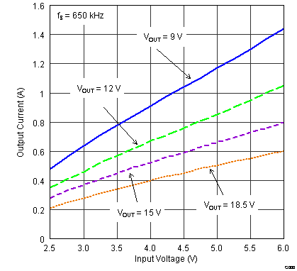
| IOUT(max) | Maximum load current | vs Input voltage at high frequency (1.2 MHz) | Figure 1 |
| vs Input voltage at low frequency (650 kHz) | Figure 2 | ||
| η | Efficiency | vs Load current, VS = 12 V, VIN = 3.3 V | Figure 3 |
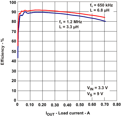
| vs Load current, VS = 9 V, VIN = 3.3 V | Figure 4 | ||
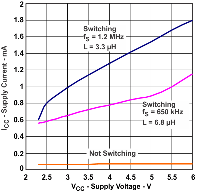
| Supply current | vs Supply voltage | Figure 5 | |
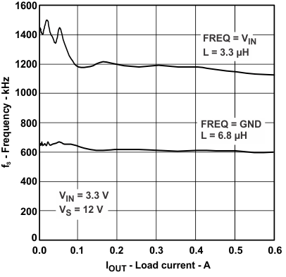
| Frequency | vs Load current | Figure 6 | |
| vs Supply voltage | Figure 7 | ||
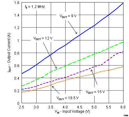 Figure 1. Maximum Load Current vs Input Voltage
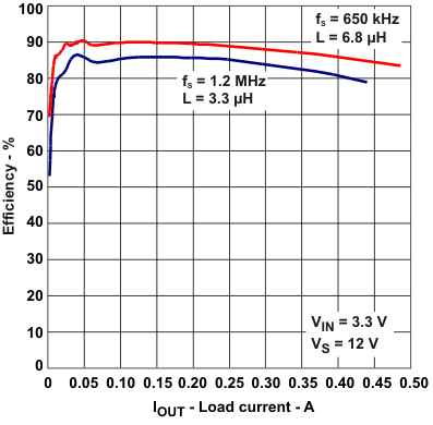 Figure 3. Efficiency vs Load Current, VS = 12 V, VIN = 3.3 V
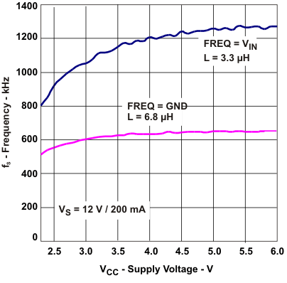 Figure 7. Frequency vs Supply Voltage
