SLVS821E May 2008 – May 2019 TPS61087
PRODUCTION DATA.
- 1 Features
- 2 Applications
- 3 Description
- 4 Revision History
- 5 Pin Configuration and Functions
- 6 Specifications
- 7 Detailed Description
- 8 Application and Implementation
- 9 Power Supply Recommendations
- 10Layout
- 11Device and Documentation Support
- 12Mechanical, Packaging, and Orderable Information
Package Options
Mechanical Data (Package|Pins)
Thermal pad, mechanical data (Package|Pins)
Orderable Information
8.3.1 General Boost Application Circuits
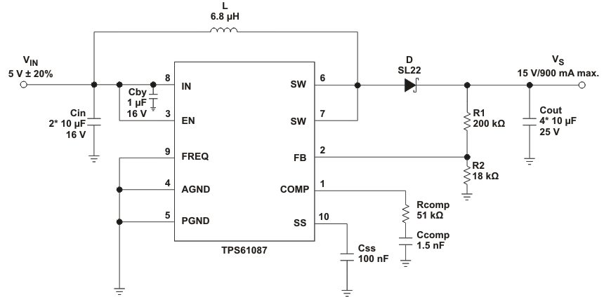 Figure 14. Typical Application, 5 V to 15 V (fS = 650 kHz)
 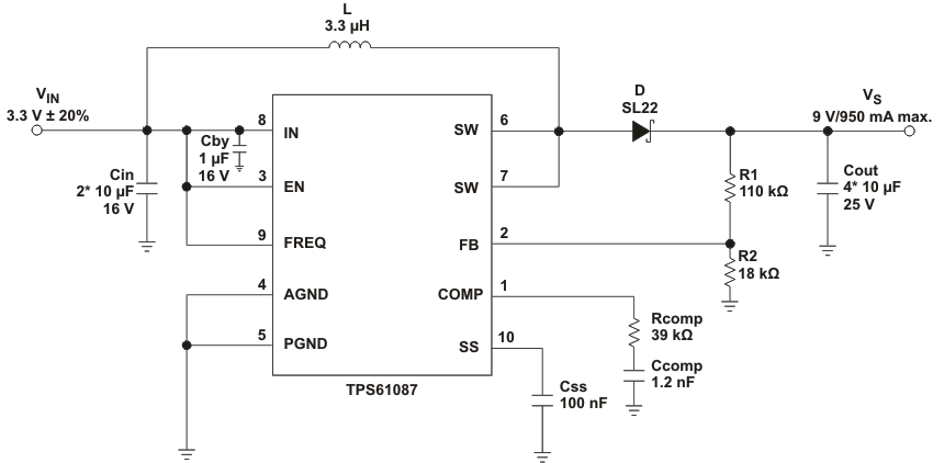 Figure 15. Typical Application, 3.3 V to 9 V (fS = 1.2 MHz)
 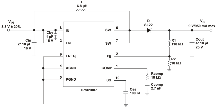 Figure 16. Typical Application, 3.3 V to 9 V (fS = 650 kHz)
 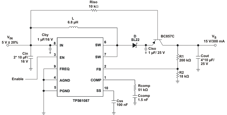 Figure 17. Typical Application With External Load Disconnect Switch
 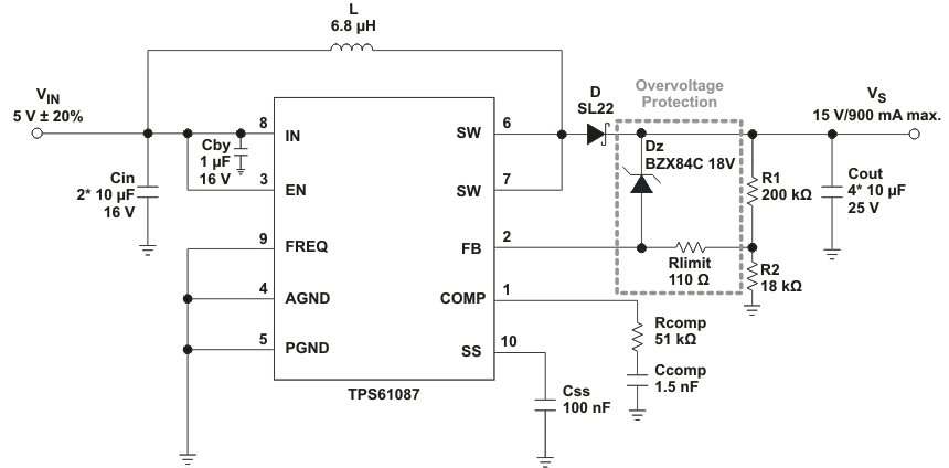 Figure 18. Typical Application, 5 V to 15 V (fS = 1.2 MHz) With Overvoltage Protection