SLVSCM8D May   2015  – August 2021 TPS61088

PRODUCTION DATA  

  1. Features
  2. Applications
  3. Description
  4. Revision History
  5. Pin Configuration and Functions
  6. Specifications
    1. 6.1 Absolute Maximum Ratings
    2. 6.2 ESD Ratings
    3. 6.3 Recommended Operating Conditions
    4. 6.4 Thermal Information
    5. 6.5 Electrical Characteristics
    6. 6.6 Typical Characteristics
  7. Detailed Description
    1. 7.1 Overview
    2. 7.2 Functional Block Diagram
    3. 7.3 Feature Description
      1. 7.3.1 Enable and Start-up
      2. 7.3.2 Undervoltage Lockout (UVLO)
      3. 7.3.3 Adjustable Switching Frequency
      4. 7.3.4 Adjustable Peak Current Limit
      5. 7.3.5 Overvoltage Protection
      6. 7.3.6 Thermal Shutdown
    4. 7.4 Device Functional Modes
      1. 7.4.1 Operation
        1. 7.4.1.1 PWM Mode
        2. 7.4.1.2 PFM Mode
  8. Application and Implementation
    1. 8.1 Application Information
    2. 8.2 Typical Application
      1. 8.2.1 Design Requirements
      2. 8.2.2 Detailed Design Procedure
        1. 8.2.2.1 Custom Design with WEBENCH Tools
        2. 8.2.2.2 Setting Switching Frequency
        3. 8.2.2.3 Setting Peak Current Limit
        4. 8.2.2.4 Setting Output Voltage
        5. 8.2.2.5 Inductor Selection
        6. 8.2.2.6 Input Capacitor Selection
        7. 8.2.2.7 Output Capacitor Selection
        8. 8.2.2.8 Loop Stability
      3. 8.2.3 Application Curves
  9. Power Supply Recommendations
  10. 10Layout
    1. 10.1 Layout Guidelines
    2. 10.2 Layout Example
    3. 10.3 Thermal Considerations
  11. 11Device and Documentation Support
    1. 11.1 Device Support
      1. 11.1.1 Third-Party Products Disclaimer
      2. 11.1.2 Development Support
        1. 11.1.2.1 Custom Design with WEBENCH Tools
    2. 11.2 Receiving Notification of Documentation Updates
    3. 11.3 Support Resources
    4. 11.4 Trademarks
    5. 11.5 Electrostatic Discharge Caution
    6. 11.6 Glossary
  12. 12Mechanical, Packaging, and Orderable Information

Package Options

Mechanical Data (Package|Pins)
Thermal pad, mechanical data (Package|Pins)
Orderable Information

Output Capacitor Selection

For small output voltage ripple, TI recommends a low-ESR output capacitor like a ceramic capacitor. Typically, three 22-μF ceramic output capacitors work for most applications. Higher capacitor values can be used to improve the load transient response. Take care when evaluating the derating of a capacitor under DC bias. The bias can significantly reduce capacitance. Ceramic capacitors can lose most of their capacitance at rated voltage. Therefore, leave margin on the voltage rating to ensure adequate effective capacitance. From the required output voltage ripple, use the following equations to calculate the minimum required effective capacitance COUT:
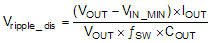
Equation 11. GUID-2CB121B7-3FC9-4919-BA88-2C2567D04E5B-low.gif
Equation 12. GUID-B0767A0F-AD1B-4A4E-8550-D243FFD219D6-low.gif

where

  • Vripple_dis is output voltage ripple caused by charging and discharging of the output capacitor
  • Vripple_ESR is output voltage ripple caused by ESR of the output capacitor
  • VIN_MIN is the minimum input voltage of boost converter
  • VOUT is the output voltage
  • IOUT is the output current
  • ILpeak is the peak current of the inductor
  • ƒSW is the converter switching frequency
  • RC_ESR is the ESR of the output capacitors