TPS6109x Synchronous Boost Converter With 2-A Switch
1 Features
- Synchronous (96% Efficient) Boost Converter With 500-mA Output Current From 1.8-V Input
- Available in a 16-Pin VQFN 4 x 4 Package
- Device Quiescent Current: 20 µA (Typ)
- Input Voltage Range: 1.8 V to 5.5 V
- Adjustable Output Voltage Up to 5.5 V Fixed Output Voltage Options
- Power Save Mode for Improved Efficiency at Low Output Power
- Low Battery Comparator
- Low EMI-Converter (Integrated Antiringing Switch)
- Load Disconnect During Shutdown
- Over-Temperature Protection
2 Applications
- All Single Cell Li or Dual Cell Battery or USB Powered Operated Products
- MP3 Player
- PDAs
- Other Portable Equipment
3 Description
The TPS6109x devices provide a power supply solution for products powered by either a one-cell Li-Ion or Li-Polymer, or a two-cell alkaline, NiCd or NiMH battery and required supply currents up to or higher than 1 A. The converter generates a stable output voltage that is either adjusted by an external resistor divider or fixed internally on the chip. It provides high efficient power conversion and is capable of delivering output currents up to 0.5 A at 5 V at a supply voltage down to 1.8 V. The implemented boost converter is based on a fixed frequency, pulse-width- modulation (PWM) controller using a synchronous rectifier to obtain maximum efficiency. Boost switch and rectifier switch are connected internally to provide the lowest leakage inductance and best EMI behavior possible. The maximum peak current in the boost switch is limited to a value of 2500 mA.
The converter can be disabled to minimize battery drain. During shutdown, the load is completely disconnected from the battery. A low-EMI mode is implemented to reduce ringing and, in effect, lower radiated electromagnetic energy when the converter enters the discontinuous conduction mode.
The output voltage can be programmed by an external resistor divider or is fixed internally on the chip.
The device is packaged in a 16-pin VQFN 4-mm x 4-mm (16 RSA) package.
Device Information(1)
| PART NUMBER | PACKAGE | BODY SIZE (NOM) |
|---|---|---|
| TPS61090 | VQFN (10) | 4.00 mm × 4.00 mm |
| TPS61091 | ||
| TPS61092 |
- For all available packages, see the orderable addendum at the end of the datasheet.
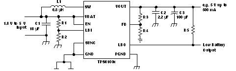
Simplified Application Schematic
4 Revision History
Changes from B Revision (April 2005) to C Revision
- Added Pin Configuration and Functions section, ESD Ratings table, Feature Description section, Device Functional Modes, Application and Implementation section, Power Supply Recommendations section, Layout section, Device and Documentation Support section, and Mechanical, Packaging, and Orderable Information section Go
5 Device Comparison Table
| TA | OUTPUT VOLTAGE DC-DC(1) | PACKAGE | PART NUMBER(2) |
|---|---|---|---|
| 40°C to 85°C | Adjustable | 16-pin VQFN 4 mm × 4 mm | TPS61090RSA |
| 3.3 V | 16-pin VQFN 4 mm × 4 mm | TPS61091RSA | |
| 5 V | 16-pin VQFN 4 mm × 4 mm | TPS61092RSA |
6 Pin Configuration and Functions

Pin Functions
| PIN | I/O | DESCRIPTION | |
|---|---|---|---|
| NAME | NO. | ||
| EN | 11 | I | Enable input. (1/VBAT enabled, 0/GND disabled) |
| FB | 14 | I | Voltage feedback of adjustable versions |
| GND | 13 | I/O | Control/logic ground |
| LBI | 9 | I | Low battery comparator input (comparator enabled with EN) |
| LBO | 12 | O | Low battery comparator output (open drain) |
| NC | 2 | Not connected | |
| PGND | 5, 6, 7 | I/O | Power ground |
| PowerPAD™ | — | — | Must be soldered to achieve appropriate power dissipation. Should be connected to PGND. |
| SYNC | 10 | I | Enable/disable power save mode (1: VBAT disabled, 0: GND enabled, clock signal for synchronization) |
| SW | 3, 4 | I | Boost and rectifying switch input |
| VBAT | 8 | I | Supply voltage |
| VOUT | 1, 15, 16 | O | DC-DC output |
7 Specifications
7.1 Absolute Maximum Ratings
over operating free-air temperature range (unless otherwise noted)(1)| MIN | MAX | UNIT | ||
|---|---|---|---|---|
| Input voltage on LBI | –0.3 | 3.6 | V | |
| Input voltage on SW, VOUT, LBO, VBAT, SYNC, EN, FB | –0.3 | 7 | V | |
| TA | Operating free air temperature | –40 | 85 | °C |
| TJ | Maximum junction temperature | 150 | °C | |
| Tstg | Storage temperature | –65 | 150 | °C |
7.2 ESD Ratings
| VALUE | UNIT | |||
|---|---|---|---|---|
| V(ESD) | Electrostatic discharge | Human-body model (HBM), per ANSI/ESDA/JEDEC JS-001(1) | ±2000 | V |
| Charged-device model (CDM), per JEDEC specification JESD22-C101(2) | ±1000 | |||
7.3 Recommended Operating Conditions
| MIN | NOM | MAX | UNIT | ||
|---|---|---|---|---|---|
| VI | Supply voltage at VBAT | 1.8 | 5.5 | V | |
| L | Inductance | 2.2 | 6.8 | µH | |
| Ci | Input, capacitance | 10 | µF | ||
| Co | Output capacitance | 22 | 100 | ||
| TA | Operating free air temperature | –40 | 85 | °C | |
| TJ | Operating virtual junction temperature | –40 | 125 |
7.4 Electrical Characteristics
over recommended free-air temperature range and over recommended input voltage range (typical values are at an ambient temperature range of 25°C) (unless otherwise noted)| PARAMETER | TEST CONDITIONS | MIN | TYP | MAX | UNIT | ||
|---|---|---|---|---|---|---|---|
| DC-DC STAGE | |||||||
| VI | Input voltage range | 1.8 | 5.5 | V | |||
| VO | TPS61090 output voltage range | 1.8 | 5.5 | ||||
| VFB | TPS61090 feedback voltage | 490 | 500 | 510 | mV | ||
| f | Oscillator frequency | 500 | 600 | 700 | kHz | ||
| Frequency range for synchronization | 500 | 700 | |||||
| ISW | Switch current limit | VOUT= 5 V | 2000 | 2200 | 2500 | mA | |
| Start-up current limit | 0.4 x ISW | ||||||
| Boost switch on resistance | VOUT= 5 V | 55 | mΩ | ||||
| Rectifying switch on resistance | VOUT= 5 V | 55 | |||||
| Total accuracy | –3% | 3% | |||||
| Line regulation | 0.6% | ||||||
| Load regulation | 0.6% | ||||||
| Quiescent current | into VBAT | IO = 0 mA, VEN = VBAT = 1.8 V, VOUT =5 V | 10 | 25 | µA | ||
| into VOUT | IO = 0 mA, VEN = VBAT = 1.8 V, VOUT = 5 V | 10 | 20 | ||||
| Shutdown current | VEN= 0 V, VBAT = 2.4 V | 0.1 | 1 | ||||
| CONTROL STAGE | |||||||
| VUVLO | Under voltage lockout threshold | VLBI voltage decreasing | 1.5 | V | |||
| VIL | LBI voltage threshold | VLBI voltage decreasing | 490 | 500 | 510 | mV | |
| LBI input hysteresis | 10 | ||||||
| LBI input current | EN = VBAT or GND | 0.01 | 0.1 | µA | |||
| LBO output low voltage | VO = 3.3 V, IOI = 100 µA | 0.04 | 0.4 | V | |||
| LBO output low current | 100 | µA | |||||
| LBO output leakage current | VLBO = 7 V | 0.01 | 0.1 | ||||
| VIL | EN, SYNC input low voltage | 0.2 × VBAT | V | ||||
| VIH | EN, SYNC input high voltage | 0.8 × VBAT | |||||
| EN, SYNC input current | Clamped on GND or VBAT | 0.01 | 0.1 | µA | |||
| Overtemperature protection | 140 | °C | |||||
7.5 Typical Characteristics
Table 1. Table of Graphs
| DC-DC Converter | Figure | ||
|---|---|---|---|
| Maximum output current | vs Input voltage | Figure 1, Figure 2 | |
| Efficiency | vs Output current (TPS61090) (VO = 2.5 V, VI = 1.8 V, VSYNC = 0 V) | Figure 3 | |
| vs Output current (TPS61091) (VO = 3.3 V, VI = 1.8 V, 2.4 V, VSYNC = 0 V) | Figure 4 | ||
| vs Output current (TPS61092) (VO = 5.0 V, VI = 2.4 V, 3.3 V, VSYNC = 0 V) | Figure 5 | ||
| vs Output current (TPS61091) (IO = 10 mA, 100 mA, 500 mA, VSYNC = 0 V) | Figure 6 | ||
| vs Output current (TPS61092) (IO = 10 mA, 100 mA, 500 mA, VSYNC = 0 V) | Figure 7 | ||
| Output voltage | vs Output current (TPS61091) (VI = 2.4 V) | Figure 8 | |
| vs Output current (TPS61092) (VI = 3.3 V) | Figure 9 | ||
| No-load supply current into VBAT | Voltage (TPS61092) | Figure 10 | |
| No-load supply current into VOUT | vs Input voltage (TPS61092) | Figure 11 | |
| Minimum Load Resistance at Start-Up | vs Input Voltage (TPS61092) (VI = 3.3 V) | Figure 12 | |
 Figure 1. TPS61091 Maximum Output Current vs Input Voltage
 Figure 3. TPS61090 Efficiency vs Output Current
 Figure 5. TPS61092 Efficiency vs Output Current
 Figure 7. TPS61092 Efficiency vs Output Current
 Figure 9. TPS61092 Output Voltage vs Output Current
 Figure 11. TPS61092 No-Load Supply Current Into VOUT vs Input Voltage
 Figure 2. TPS61092 Maximum Output Current vs Input Voltage
 Figure 4. TPS61091 Efficiency vs Output Current
 Figure 6. TPS61091 Efficiency vs Output Current
 Figure 8. TPS61091 Efficiency vs Output Current
 Figure 10. TPS61092 No-Load Supply Current Into VBAT Voltage
 Figure 12. Minimum Load Resistance at Start-Up vs Input Voltage
8 Parameter Measurement Information
 Figure 13. Parameter Schematic