SLVSCO6 January 2015 TPS61093-Q1
PRODUCTION DATA.
- 1 Features
- 2 Applications
- 3 Description
- 4 Simplified Schematic
- 5 Revision History
- 6 Pin Configuration and Functions
- 7 Specifications
- 8 Detailed Description
- 9 Application and Implementation
- 10Power Supply Recommendations
- 11Layout
- 12Device and Documentation Support
- 13Mechanical, Packaging, and Orderable Information
Package Options
Mechanical Data (Package|Pins)
- DSK|10
Thermal pad, mechanical data (Package|Pins)
- DSK|10
Orderable Information
9 Application and Implementation
9.1 Application Information
The following section provides a step-by-step design approach for configuring the TPS61093-Q1 as a voltage regulating boost converter, as shown in Figure 6.
9.2 Typical Applications
9.2.1 15V Output Boost Converter
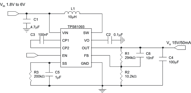 Figure 6. 15V Boost Converter with 100µF Output Capacitor
9.2.1.1 Design Requirements
Table 2. Design Parameters
| PARAMETERS | VALUES |
|---|---|
| Input voltage | 4.2 V |
| Output voltage | 15 V |
| Operating frequency | 1.2 MHz |
9.2.1.2 Detailed Design Procedure
9.2.1.2.1 Output Program
To program the output voltage, select the values of R1 and R2 (see Figure 7) according to Equation 1.
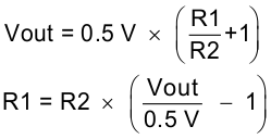
A recommended value for R2 is approximately 10-kΩ which sets the current in the resistor divider chain to 0.5V/10kΩ = 50-μA. The output voltage tolerance depends on the VFB accuracy and the resistor divider.
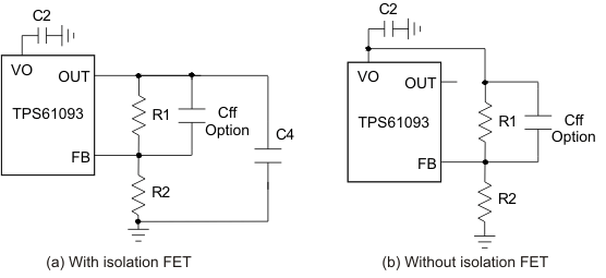 Figure 7. Resistor Divider to Program Output Voltage
9.2.1.2.2 Without Isolation FET
The efficiency of the TPS61093-Q1 can be improved by connecting the load to the VO pin instead of the OUT pin. The power loss in the isolation FET is then negligible, as shown in Figure 8. The tradeoffs when bypassing the isolation FET are:
- Leakage path between input and output causes the output to be a diode drop below the input voltage when the IC is in shutdown
- No overload circuit protection
When the load is connected to the VO pin, the output capacitor on the VO pin should be above 1-μF.
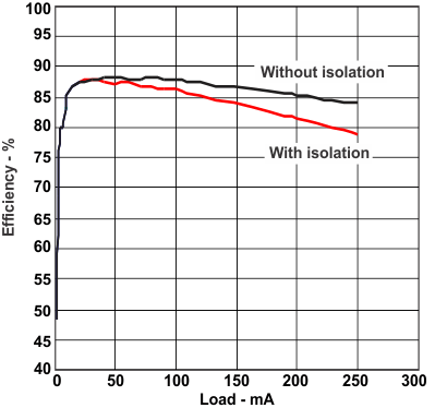 Figure 8. Efficiency vs. Load
9.2.1.2.3 Start Up
The TPS61093-Q1 turns on the isolation FET and PWM switch when the EN pin is pulled high. During the soft start period, the R and C network on the SS pin is charged by an internal bias current of 5-μA (typ). The RC network sets the reference voltage ramp up slope. Since the output voltage follows the reference voltage via the FB pin, the output voltage rise time follows the SS pin voltage until the SS pin voltage reaches 0.5-V. The soft start time is given by Equation 2.

where
- C5 is the capacitor connected to the SS pin
When the EN pin is pulled low to switch the IC off, the SS pin voltage is discharged to zero by the resistor R3. The discharge period depends on the RC time constant. Note that if the SS pin voltage is not discharged to zero before the IC is enabled again, the soft start circuit may not slow the output voltage startup and may not reduce the startup inrush current.
9.2.1.2.4 Switch Duty Cycle
The maximum switch duty cycle (D) of the TPS61093-Q1 is 90% (minimum). The duty cycle of a boost converter under continuous conduction mode (CCM) is given by:

The duty cycle must be lower than the specification in the application; otherwise the output voltage cannot be regulated.
The TPS61093-Q1 has a minimum ON pulse width once the PWM switch is turned on. As the output current drops, the device enters discontinuous conduction mode (DCM). If the output current drops extremely low, causing the ON time to be reduced to the minimum ON time, the TPS61093-Q1 enters pulse-skipping mode. In this mode, the device keeps the power switch off for several switching cycles to keep the output voltage in regulation. See Figure 14. The output current when the IC enters skipping mode is calculated with Equation 4.

where
- Tmin_on = Minimum ON pulse width specification (typically 65-ns);
- L = Selected inductor value;
- fSW = Converter switching frequency (typically 1.2-MHz)
9.2.1.2.5 Inductor Selection
Because the selection of the inductor affects steady state operation, transient behavior, and loop stability, the inductor is the most important component in power regulator design. There are three important inductor specifications, inductor value, saturation current, and dc resistance. Considering inductor value alone is not enough.
The saturation current of the inductor should be higher than the peak switch current as calculated in Equation 5.
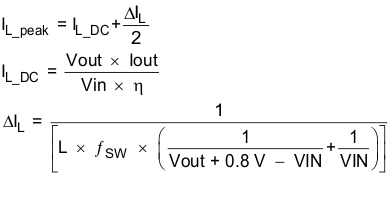
where
- IL_peak = Peak switch current
- IL_DC = Inductor average current
- ΔIL = Inductor peak to peak current
- η = Estimated converter efficiency
Normally, it is advisable to work with an inductor peak-to-peak current of less than 30% of the average inductor current. A smaller ripple from a larger valued inductor reduces the magnetic hysteresis losses in the inductor and EMI. But in the same way, load transient response time is increased. Also, the inductor value should not be outside the 2.2-μH to 10-μH range in the recommended operating conditions table. Otherwise, the internal slope compensation and loop compensation components are unable to maintain small signal control loop stability over the entire load range. Table 3 lists the recommended inductor for the TPS61093-Q1.
Table 3. Recommended Inductors for the TPS61093-Q1
| Part Number | L (μH) | DCR Max (mΩ) | Saturation Current (A) | Size (L×W×H mm) | Vendor |
|---|---|---|---|---|---|
| #A915_Y-4R7M | 4.7 | 45 | 1.5 | 5.2x5.2x3.0 | Toko |
| #A915_Y-100M | 10 | 90 | 1.09 | 5.2x5.2x3.0 | Toko |
| VLS4012-4R7M | 4.7 | 132 | 1.1 | 4.0x4.0x1.2 | TDK |
| VLS4012-100M | 10 | 240 | 0.82 | 4.0x4.0x1.2 | TDK |
| CDRH3D23/HP | 10 | 198 | 1.02 | 4.0x4.0x2.5 | Sumida |
| LPS5030-103ML | 10 | 127 | 1.4 | 5.0x5.0x3.0 | Coilcraft |
9.2.1.2.6 Input And Output Capacitor Selection
The output capacitor is mainly selected to meet the requirements for output ripple and loop stability. This ripple voltage is related to the capacitor’s capacitance and its equivalent series resistance (ESR). Assuming a ceramic capacitor with zero ESR, the minimum capacitance needed for a given ripple can be calculated by:

where
- Vripple = peak to peak output ripple
The ESR impact on the output ripple must be considered if tantalum or electrolytic capacitors are used.
Care must be taken when evaluating a ceramic capacitor’s derating under dc bias, aging, and ac signal. For example, larger form factor capacitors (in 1206 size) have their self resonant frequencies in the range of the switching frequency. So the effective capacitance is significantly lower. The dc bias can also significantly reduce capacitance. A ceramic capacitor can lose as much as 50% of its capacitance at its rated voltage. Therefore, always leave margin on the voltage rating to ensure adequate capacitance at the required output voltage.
A 4.7-μF (minimum) input capacitor is recommended. The output requires a capacitor in the range of 1 μF to 10 μF. The output capacitor affects the small signal control loop stability of the boost regulator. If the output capacitor is below the range, the boost regulator can potentially become unstable.
The popular vendors for high value ceramic capacitors are:
9.2.1.2.7 Small Signal Stability
The TPS61093-Q1 integrates slope compensation and the RC compensation network for the internal error amplifier. Most applications will be control loop stable if the recommended inductor and input/output capacitors are used. For those few applications that require components outside the recommended values, the internal error amplifier’s gain and phase are presented in Figure 9.
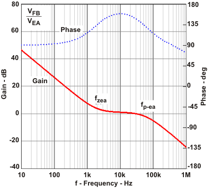 Figure 9. Bode Plot of Error Amplifier Gain and Phase
The RC compensation network generates a pole fp-ea of 57-kHz and a zero fz-ea of 1.9-kHz, shown in Figure 9. Use Equation 7 to calculate the output pole, fP, of the boost converter. If fP << fz-ea. due to a large capacitor beyond 10 μF, for example, a feed forward capacitor on the resistor divider, as shown in Figure 9, is necessary to generate an additional zero fz-f. to improve the loop phase margin and improve the load transient response. The low frequency pole fp-f and zero fz-f generated by the feed forward capacitor are given by Equation 8 and Equation 9:


where
- Cff = the feed-forward capacitor
For example, in the typical application circuitry (see Figure 7), the output pole fP is approximately 1-kHz. When the output capacitor is increased to 100-μF, then the fP is reduced to 10-Hz. Therefore, a feed-forward capacitor of 10-nF compensates for the low frequency pole.
A feed forward capacitor that sets fz-f near 10-kHz improves the load transient response in most applications, as shown in Figure 11.
9.2.1.3 Application Curves
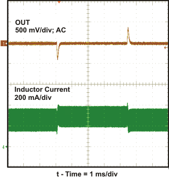 Figure 10. 3.3V to 3.6V Line Transient Response
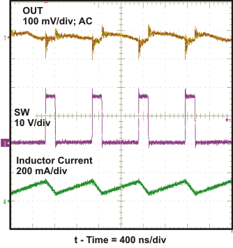 Figure 12. PWM Control in CCM
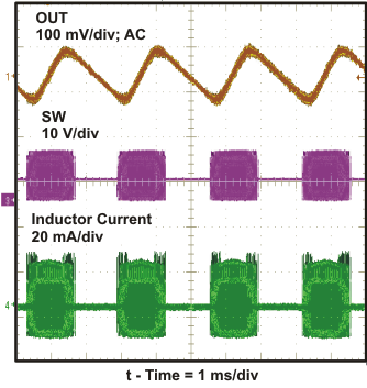 Figure 14. Pulse Skip Mode at Light Load
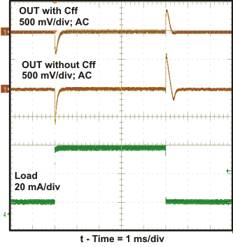 Figure 11. 10mA to 50mA Load Transient Response
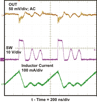 Figure 13. PWM Control in DCM
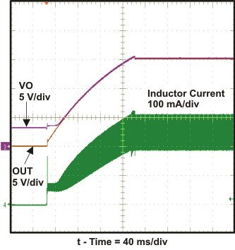 Figure 15. Soft Start-Up
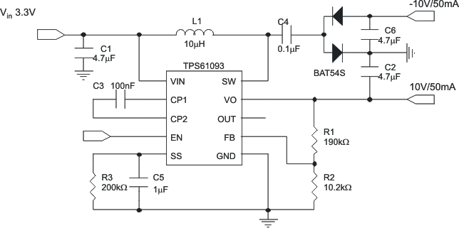
9.2.2 10 V, –10 V Dual Output Boost Converter
9.2.2.1 Design Requirements
Table 4. Design Parameters
| PARAMETERS | VALUES |
|---|---|
| Input voltage | 3.3 V |
| Output voltage | 10 V/–10 V |
| Operating frequency | 1.2 MHz |
9.2.2.2 Detailed Design Procedure
Refer to Detailed Design Procedure for the 15V Output Boost Converter.
9.2.2.3 Application Curves
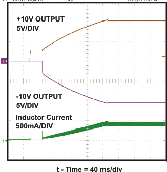 Figure 16. Soft Startup Waveform, 10 V, -10 V Dual Output Boost Converter