SLVS992D September   2009  – April 2019 TPS61093

PRODUCTION DATA.  

  1. Features
  2. Applications
  3. Description
    1.     Device Images
      1.      Simplified Schematic
  4. Revision History
  5. Pin Configuration and Functions
    1.     Pin Functions
  6. Specifications
    1. 6.1 Absolute Maximum Ratings
    2. 6.2 ESD Ratings
    3. 6.3 Recommended Operating Conditions
    4. 6.4 Thermal Information
    5. 6.5 Electrical Characteristics
    6. 6.6 Typical Characteristics
  7. Detailed Description
    1. 7.1 Overview
    2. 7.2 Functional Block Diagram
    3. 7.3 Feature Description
      1. 7.3.1 Shutdown and Load Discharge
      2. 7.3.2 Overload and Overvoltage Protection
      3. 7.3.3 UVLO
      4. 7.3.4 Thermal Shutdown
    4. 7.4 Device Functional Modes
  8. Application and Implementation
    1. 8.1 Application Information
    2. 8.2 Typical Applications
      1. 8.2.1 15 V Output Boost Converter
        1. 8.2.1.1 Design Requirements
        2. 8.2.1.2 Detailed Design Procedure
          1. 8.2.1.2.1 Custom Design With WEBENCH® Tools
          2. 8.2.1.2.2 Output Program
          3. 8.2.1.2.3 Without Isolation FET
          4. 8.2.1.2.4 Start-Up
          5. 8.2.1.2.5 Switch Duty Cycle
          6. 8.2.1.2.6 Inductor Selection
          7. 8.2.1.2.7 Input and Output Capacitor Selection
          8. 8.2.1.2.8 Small Signal Stability
        3. 8.2.1.3 Application Curves
      2. 8.2.2 10 V, –10 V Dual Output Boost Converter
        1. 8.2.2.1 Design Requirements
        2. 8.2.2.2 Detailed Design Procedure
        3. 8.2.2.3 Application Curve
  9. Power Supply Recommendations
  10. 10Layout
    1. 10.1 Layout Guidelines
    2. 10.2 Layout Example
  11. 11Device and Documentation Support
    1. 11.1 Device Support
      1. 11.1.1 Third-Party Products Disclaimer
      2. 11.1.2 Development Support
        1. 11.1.2.1 Custom Design With WEBENCH® Tools
    2. 11.2 Receiving Notification of Documentation Updates
    3. 11.3 Community Resources
    4. 11.4 Trademarks
    5. 11.5 Electrostatic Discharge Caution
    6. 11.6 Glossary
  12. 12Mechanical, Packaging, and Orderable Information

Package Options

Mechanical Data (Package|Pins)
Thermal pad, mechanical data (Package|Pins)
Orderable Information

Output Program

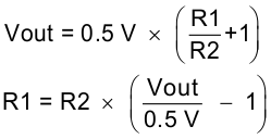
To program the output voltage, select the values of R1 and R2 (see Figure 7) according to Equation 1.

Equation 1. TPS61093 eq3_vout_lvs992.gif

A recommended value for R2 is approximately 10 kΩ which sets the current in the resistor divider chain to 0.5 V/10 kΩ = 50 μA. The output voltage tolerance depends on the VFB accuracy and the resistor divider.
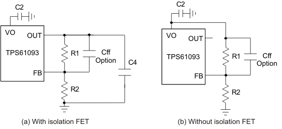
TPS61093 res_div_lvs992.gifFigure 7. Resistor Divider to Program Output Voltage