SLVSFH6C January 2021 – December 2021 TPS61094
PRODUCTION DATA
- 1 Features
- 2 Applications
- 3 Description
- 4 Revision History
- 5 Pin Configuration and Functions
- 6 Specifications
- 7 Detailed Description
- 8 Application and Implementation
- 9 Power Supply Recommendations
- 10Layout
- 11Device and Documentation Support
- 12Mechanical, Packaging, and Orderable Information
Package Options
Mechanical Data (Package|Pins)
- DSS|12
Thermal pad, mechanical data (Package|Pins)
- DSS|12
Orderable Information
7.4.5.1 Three States (Boost_on, Buck_on, and Supplement) Transition
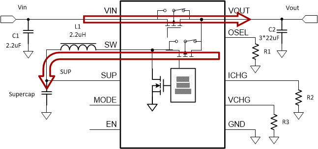
In Auto buck or Boost mode operation, there are three states: boost_on, buck_on, and supplement, as shown in Figure 7-2 to Figure 7-4. The boost_on state occurs when the bypass switch is turned off and the TPS61094 works in Boost mode to regulate output voltage to the OSEL setting. The buck_on state occurs when the bypass switch is turned on and the TPS61094 works in Buck mode, charging the SUP pin by an input source according to the charging current and termination voltage settings at the ICHG and VCHG pin in this situation, which is similar to the Forced buck mode operation. Supplement mode is the intermediate state when the TPS61094 transfers between boost_on and buck_on opetation. In Supplement mode, Boost mode is active and the bypass MOSFET operates as an LDO, the VIN and SUP power source supply the output load together.
 Figure 7-2 Typical
Boost_on State Circuit
 Figure 7-3 Typical
Buck_on State Circuit
 Figure 7-4 Typical
Supplement State Circuit
Figure 7-4 Typical
Supplement State CircuitThe TPS61094 can automatically transfer in these three states based on input voltage and output voltage, as shown in Figure 7-5.
 Figure 7-5 Three
States(Boost_on, Buck_on, and Supplement) Transition
 Path 1: The TPS61094 works at buck_on state first. There is a heavy load transient in the output load and the input source cannot hold it, which makes the output voltage lower than the output target voltage (OSEL pin setting). The TPS61094 transfers from buck_on to supplement state. Input and SUP power source can supply the heavy load together.
Path 2: In supplement state, if the input voltage is higher than the output target voltage + 100 mV and the output voltage is higher than the output target voltage, meaning the input power source can support the output load, the TPS61094 transfers from supplement to buck_on state.
Path 3: In supplement operation, if the output load is light, the output voltage is higher than the output target voltage. The TPS61094 transfers from supplement to boost_on state. The TPS61094 has approximately 60-nA IQ in Boost mode, which can help the system has higher efficiency at light load.
Path 4: In boost_on state, when the input power source is higher than the output target voltage + 100 mV, the TPS61094 transfers from boost_on to supplement state.
Path 5: A quick way to transfer from buck_on to boost_on state. At buck_on state, if the load is light and input voltage is lower than the output target voltage + 100 mV, the TPS61094 can enter boost_on state.
In boost_on mode, when the SUP pin voltage is higher than output target voltage, the TPS61094 enters Pass-through mode. The TPS61094 stops switching and fully turns on high-side MOSFET. The devices stays in boost_on (Pass-through mode) until the SUP pin voltage is lower than the output target voltage.