SLVSC26B November 2013 – May 2024 TPS61162A , TPS61163A
PRODUCTION DATA
- 1
- 1 Features
- 2 Applications
- 3 Description
- 4 Pin Configuration and Functions
- 5 Specifications
- 6 Detailed Description
- 7 Application and Implementation
- 8 Device and Documentation Support
- 9 Revision History
- 10Mechanical, Packaging, and Orderable Information
Package Options
Mechanical Data (Package|Pins)
- YFF|9
Thermal pad, mechanical data (Package|Pins)
Orderable Information
6.4.1 One-Wire Digital Interface (EasyScale Interface)
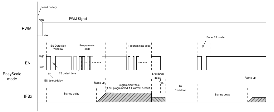
The EN pin features a simple digital interface to allow digital brightness control. The digital dimming interface can save the processor power and battery life as it does not require PWM signals all the time, and the processor can enter idle mode if possible. In order to enable the EasyScale interface, the following conditions must be satisfied, and the specific digital pattern on the EN pin must be recognized by the device every time the TPS61162A, TPS61163A starts up from shutdown mode.
- VIN voltage is higher than UVLO threshold, and PWM pin is pulled high.
- Pull EN pin from low to high to enable the TPS61162A, TPS61163A. At this moment, the EasyScale detection window starts.
- After EasyScale detection delay time (tes_delay, 100µs), drive EN to low for more than EasyScale detection time (tes_detect, 260µs).
The third step must be finished before the EasyScale detection window (tes_win, 1ms) expires, and once this step is finished, the EasyScale interface is enabled, and the EasyScale communication can start. Refer to Figure 6-3 for a graphical explanation.
 Figure 6-3 Easyscale
Interface Detection
Figure 6-3 Easyscale
Interface DetectionThe TPS61162A, TPS61163A support 9-bit brightness code programming. By the EasyScale interface, a master can program the 9-bit code D8(MSB) to D0(LSB) to any of 511 steps with a single command. The default code value of D8~D0 is “111111111” when the device is first enabled, and the programmed value will be stored in an internal register and set the dual-channel current according to Equation 2. The code will be reset to default value when the device is shut down or disabled.

where
- IFB_full: the full-scale LED current set by the RISET at ISET pin.
- Code: the 9-bit brightness code D8~D0 programmed by EasyScale interface
When the one-wire digital interface at EN pin is selected, the PWM pin can be connected to either the VIN pin or a GPIO (refer to Section 7.2.4). If PWM pin is connected to VIN pin, EN pin alone can enable and disable the device — pulling EN pin low for more than 2.5ms disables the device; if PWM pin is connected to a GPIO, both PWM and EN signals should be high to enable the device, and either pulling EN pin low for more than 2.5ms or pulling PWM pin low for more than 20ms disables the device.