SNVSA40B October   2014  – June 2024 TPS61169

PRODUCTION DATA  

  1.   1
  2. Features
  3. Applications
  4. Description
  5. Pin Configuration and Functions
  6. Specifications
    1. 5.1 Absolute Maximum Ratings
    2. 5.2 ESD Ratings
    3. 5.3 Recommended Operating Conditions
    4. 5.4 Thermal Information
    5. 5.5 Electrical Characteristics
    6. 5.6 Typical Characteristics
  7. Detailed Description
    1. 6.1 Overview
    2. 6.2 Functional Block Diagram
    3. 6.3 Feature Description
      1. 6.3.1 Soft Start-Up
      2. 6.3.2 Open LED Protection
      3. 6.3.3 Shutdown
      4. 6.3.4 Current Program
      5. 6.3.5 LED Brightness Dimming
      6. 6.3.6 Undervoltage Lockout
      7. 6.3.7 Thermal Foldback and Thermal Shutdown
    4. 6.4 Device Functional Modes
      1. 6.4.1 Operation With CTRL
  8. Application and Implementation
    1. 7.1 Application Information
    2. 7.2 Typical Application
      1. 7.2.1 Design Requirements
      2. 7.2.2 Detailed Design Procedure
        1. 7.2.2.1 Inductor Selection
        2. 7.2.2.2 Schottky Diode Selection
        3. 7.2.2.3 Output Capacitor Selection
        4. 7.2.2.4 LED Current Set Resistor
        5. 7.2.2.5 Thermal Considerations
    3. 7.3 Application Curves
    4. 7.4 Power Supply Recommendations
    5. 7.5 Layout
      1. 7.5.1 Layout Guidelines
      2. 7.5.2 Layout Example
  9. Device and Documentation Support
    1. 8.1 Device Support
    2. 8.2 Receiving Notification of Documentation Updates
    3. 8.3 Support Resources
    4. 8.4 Trademarks
    5. 8.5 Electrostatic Discharge Caution
    6. 8.6 Glossary
  10. Revision History
  11. 10Mechanical, Packaging, and Orderable Information

Package Options

Mechanical Data (Package|Pins)
Thermal pad, mechanical data (Package|Pins)
Orderable Information

Application Curves

Typical application condition is as in Figure 7-1, VIN = 3.6V, RSET = 10.2Ω, L = 4.7µH, COUT = 1µF, 10 LEDs in series (unless otherwise specified).
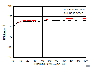
Typical application condition is as in Figure 7-1, VIN = 3.6V, RSET = 10.2Ω, L = 4.7µH, COUT = 1µF, 10 LEDs in series (unless otherwise specified).TPS61169 Efficiency vs Dimming Duty Cycle
Figure 7-2 Efficiency vs Dimming Duty Cycle. Typical application condition is as in Figure 7-1, VIN = 3.6V, RSET = 10.2Ω, L = 4.7µH, COUT = 1µF, 10 LEDs in series (unless otherwise specified).
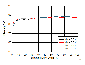
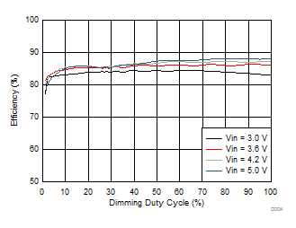
TPS61169 Efficiency vs Dimming Duty Cycle
8 LEDs in series
Figure 7-4 Efficiency vs Dimming Duty Cycle
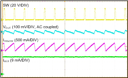
TPS61169 Switching-Dimming Duty = 100%
Time = 1µs/DIV
Figure 7-6 Switching-Dimming Duty = 100%
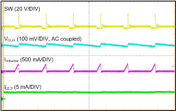
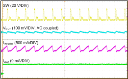
TPS61169 Switching-Dimming Duty = 10%
Time = 2µs/DIV
Figure 7-8 Switching-Dimming Duty = 10%
TPS61169 Start-Up Dimming Duty =
                        50%
Time = 2ms/DIV
Figure 7-10 Start-Up Dimming Duty = 50%
TPS61169 Shutdown Dimming
Time = 2ms/DIV
Duty = 50%
Figure 7-12 Shutdown Dimming
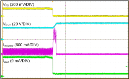
TPS61169 Open
                        LED Protection
Time = 50µs/DIV
Figure 7-14 Open LED Protection
TPS61169 Efficiency vs Dimming Duty Cycle
10 LEDs in series
Figure 7-3 Efficiency vs Dimming Duty Cycle
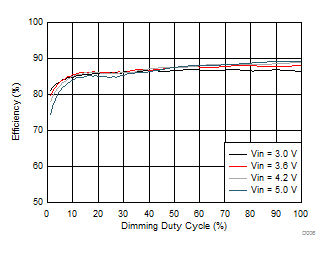
TPS61169 Efficiency vs Dimming Duty Cycle
6 LEDs in series
Figure 7-5 Efficiency vs Dimming Duty Cycle
TPS61169 Switching-Dimming Duty = 50%
Time = 1µs/DIV
Figure 7-7 Switching-Dimming Duty = 50%
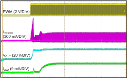
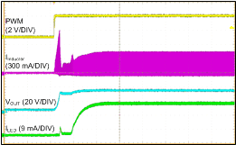
TPS61169 Start-Up Dimming Duty =
                        100%
Time = 2ms/DIV
Figure 7-9 Start-Up Dimming Duty = 100%
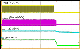
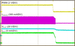
TPS61169 Shutdown Dimming Duty = 100%
Time = 2ms/DIV
Figure 7-11 Shutdown Dimming Duty = 100%
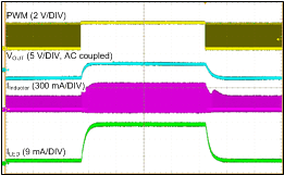
TPS61169 Dimming Transient-Dimming
Time = 5ms/DIV
Duty = 1%-100%-1%
Figure 7-13 Dimming Transient-Dimming