SLVSAX2B September 2011 – June 2020 TPS61170-Q1
PRODUCTION DATA.
- 1 Features
- 2 Applications
- 3 Description
- 4 Revision History
- 5 Pin Configuration and Functions
- 6 Specifications
- 7 Detailed Description
-
8 Application and Implementation
- 8.1 Application Information
- 8.2 Typical Applications
- 9 Power Supply Recommendations
- 10Layout
- 11Device and Documentation Support
- 12Mechanical, Packaging, and Orderable Information
Package Options
Mechanical Data (Package|Pins)
- DRV|6
Thermal pad, mechanical data (Package|Pins)
- DRV|6
Orderable Information
7.4.1 PWM Program Mode
When the CTRL pin is constantly high, the FB voltage is regulated to 1.229 V typically. However, the CTRL pin allows a PWM signal to lower this regulation voltage. The relationship between the duty cycle and FB voltage is given in Equation 1:

where
- Duty = duty cycle of the PWM signal
- 1.229 V = internal reference voltage
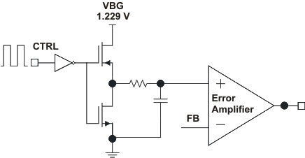
As shown in Figure 11, the IC chops up the internal 1.229-V reference voltage at the duty cycle of the PWM signal. The pulse signal is then filtered by an internal low-pass filter. The output of the filter is connected to the error amplifier as the reference voltage for the FB pin regulation. The regulation voltage is independent of the PWM logic voltage level which often has large variations.
For optimum performance, use the PWM mode in the range of 5 kHz to 100 kHz. The requirement of minimum frequency comes from the EasyScale detection delay and detection time specification for the mode selection. The device can mistakenly enter 1-wire mode if the PWM signal frequency is less than 5 kHz. Because there is an internal fixed ON-time error of 40 nS, the FB voltage absolute value will be different than expected when the PWM frequency is above 100 kHz. For example, the additional duty cycle of 3.2% due to the ON-time error increases the FB voltage when using an 800-kHz PWM signal. A compromise between PWM frequency and FB voltage accuracy extends the frequency range. Adding an external RC filter to the pin serves no purpose.
 Figure 11. Block Diagram of Programmable FB Voltage Using PWM Signal