-
TPS61177A WLED Driver for Notebooks With PWM Interface and Mixed Dimming Mode
- 1 Features
- 2 Applications
- 3 Description
- 4 Revision History
- 5 Pin Configuration and Functions
- 6 Specifications
-
7 Detailed Description
- 7.1 Overview
- 7.2 Functional Block Diagram
- 7.3
Feature Description
- 7.3.1 Supply Voltage
- 7.3.2 Boost Regulator
- 7.3.3 Programmable Switch Frequency and Slew Rate
- 7.3.4 LED Current Sinks
- 7.3.5 Enable and Start-Up Timing
- 7.3.6 Input Undervoltage Protection (UVLO)
- 7.3.7 Overvoltage Protection (OVP)
- 7.3.8 Current-Sink Open Protection
- 7.3.9 Overcurrent Protection
- 7.3.10 Thermal Protection
- 7.4 Device Functional Modes
- 7.5 Programming
- 7.6
Register Maps
- 7.6.1 MODE (A0h)
- 7.6.2 CS (A1h)
- 7.6.3 UVLO (A2h)
- 7.6.4 FREQ (A3h)
- 7.6.5 SR (A4h)
- 7.6.6 ILIM (A5h)
- 7.6.7 Control (FFh)
- 7.6.8 Example - Writing to a Single RAM Register
- 7.6.9 Example - Writing to Multiple RAM Registers
- 7.6.10 Example - Saving Contents of all RAM Registers to E2PROM
- 7.6.11 Example - Reading from a Single RAM Register
- 7.6.12 Example - Reading from a Single E2PROM Register
- 7.6.13 Example - Reading from Multiple RAM Registers
- 7.6.14 Example - Reading from Multiple E2PROM Registers
- 8 Application and Implementation
- 9 Power Supply Recommendations
- 10Layout
- 11Device and Documentation Support
- 12Mechanical, Packaging, and Orderable Information
- IMPORTANT NOTICE
Package Options
Mechanical Data (Package|Pins)
- RGR|20
Thermal pad, mechanical data (Package|Pins)
- RGR|20
Orderable Information
TPS61177A WLED Driver for Notebooks With PWM Interface and Mixed Dimming Mode
1 Features
- 2.5-V to 24-V Input Voltage Range
- 39-V Maximum Output Voltage
- Integrated 1.8-A, 40-V MOSFET
- 450-kHz to 1.2-MHz Programmable Switching Frequency
- Adaptive Boost Output to WLED Voltages
- 100-Hz to 25-kHz Wide Input PWM Dimming Frequency Range
- 1% Minimum Dimming Duty Cycle
- Small External Components
- Integrated Loop Compensation
- Six Current Sinks of 30 mA Maximum
- 1% (Typical) Current Matching
- Input PWM Glitch Filter
- PWM Brightness Interface Control
- Three Optional Dimming Methods, including Direct PWM Dimming, Analog Dimming, and Analog and PWM Mixed Dimming
- Built-in WLED Open Protection
- Thermal Shutdown
2 Applications
- Notebook and Tablet LCD Display Backlights
- Patient Monitors
- Medical Displays
- HMI
- Test and Measurement Equipment
3 Description
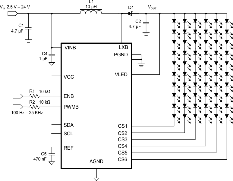
The TPS61177A device provides a highly integrated white LED (WLED) driver solution for notebook LCD backlight. This device has a built-in high-efficiency boost regulator with integrated 1.8-A, 40-V power MOSFET. The six current sink regulators provide high precision current regulation and matching. In total, the device can support up to 72 WLEDs. In addition, the boost output automatically adjusts its voltage to the WLED forward voltage to optimize efficiency.
The TPS61177A supports the analog dimming, analog and PWM dimming, and direct PWM dimming method. During analog dimming mode, each CS current linearly varies depending on the duty cycle information on the PWMB pin. During analog and PWM mixed dimming mode, the input PWM duty cycle information is translated to an analog signal to control the WLED current linearly over 25% to 100% brightness area. The device also allows adding PWM dimming when the analog current is down to 25%. Below 25%, the analog signal translates to PWM duty cycle information to control the on or off of WLED current and averages the WLED current down to 1%. The frequency of adding PWM dimming is same to input PWM frequency on the PWMB pin. While the TPS61177A also supports a direct PWM dimming method, in direct PWM dimming mode the WLED current is turned on or off, synchronized with the input PWM signal.
Device Information(1)
| PART NUMBER | PACKAGE | BODY SIZE (NOM) |
|---|---|---|
| TPS61177A | VQFN (20) | 3.50 mm x 3.50 mm |
- For all available packages, see the orderable addendum at the end of the data sheet.
Typical Application – Analog and PWM Mixed Mode
5 Pin Configuration and Functions
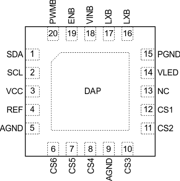
Pin Functions
| PIN | TYPE | DESCRIPTION | |
|---|---|---|---|
| NAME | NUMBER | ||
| AGND | 5, 9 | — | Signal ground of the device. |
| CS1, CS2, CS3, CS4, CS5, CS6 | 6, 7, 8, 10, 11, 12 | I | Current sink regulation inputs. They are connected to the cathode of WLEDs. The PWM loop regulates the lowest VCS to 500 mV. Each channel is limited to 30-mA current. Connect any unused CS pin to AGND or leave it open. |
| ENB | 19 | I | Enable pin |
| LXB | 16, 17 | I | Drain connection of the internal PWM switch MOSFET and external Schottky diode. |
| REF | 4 | O | The reference pin for internal error amplifier. Connect a 470-nF ceramic capacitor to REF. |
| PGND | 15 | — | Power ground of the IC. Internally, it connects to the source of the PWM switch. Tie the ground of power stage components to this ground. |
| PWMB | 20 | I | Dimming control logic input. The dimming frequency range is from 100 Hz to 25 kHz. |
| SCL | 2 | I | Clock input for I2C interface |
| SDA | 1 | I/O | Data input for I2C interface |
| VCC | 3 | I | Internal pre-regulator and supply rail for the internal logic. Do not connect any capacitor to VCC pin. |
| VINB | 18 | I | Power supply to the IC |
| VLED | 14 | I | The voltage detect pin for VOUT. |
6 Specifications
6.1 Absolute Maximum Ratings
over operating free-air temperature range (unless otherwise noted) (1)| MIN | MAX | UNIT | ||
|---|---|---|---|---|
| Voltage(2) | VINB | –0.3 | 26.4 | V |
| LXB, VLED, CS1, CS2, CS3, CS4, CS5, CS6 | –0.3 | 40 | ||
| ENB, PWMB | –0.3 | 30 | ||
| SDA, SCL, VCC | –0.3 | 3.6 | ||
| Continuous power dissipation | See Thermal Information | °C | ||
| Operating junction temperature | –40 | 150 | ||
| Storage temperature, Tstg | –65 | 150 | ||
6.2 ESD Ratings
| VALUE | UNIT | |||
|---|---|---|---|---|
| V(ESD) | Electrostatic discharge | Human-body model (HBM), per ANSI/ESDA/JEDEC JS-001(1) | ±2000 | V |
| Charged-device model (CDM), per JEDEC specification JESD22-C101(2) | ±1000 | |||
6.3 Recommended Operating Conditions
over operating free-air temperature range (unless otherwise noted)| MIN | MAX | UNIT | ||
|---|---|---|---|---|
| VIN | Input voltage | 2.5 | 24 | V |
| VOUT | Output voltage | VIN + 2 | 39 | |
| FPWM_I | PWM input signal frequency | 0.1 | 25 | kHz |
| DMIN_I | PWM input signal minimum duty cycle | 1% | ||
| FBOOST | Boost regulator switching frequency | 450 | 1200 | kHz |
| TA | Operating free-air temperature | –40 | 85 | °C |
| TJ | Operating junction temperature | –40 | 125 | |
6.4 Thermal Information
| THERMAL METRIC(1) | TPS61177A | UNIT | |
|---|---|---|---|
| RGR (VQFN) | |||
| 20 PINS | |||
| RθJA | Junction-to-ambient thermal resistance | 34.4 | °C/W |
| RθJC(top) | Junction-to-case (top) thermal resistance | 46.8 | °C/W |
| RθJB | Junction-to-board thermal resistance | 12.2 | °C/W |
| ψJT | Junction-to-top characterization parameter | 0.5 | °C/W |
| ψJB | Junction-to-board characterization parameter | 12.3 | °C/W |
| RθJC(bot) | Junction-to-case (bottom) thermal resistance | 1.0 | °C/W |
6.5 Electrical Characteristics
VINB = 12 V, PWMB/ENB = logic high, CS current = 20 mA, CS voltage = 500 mV, TA = –40°C to +85°C, typical values are at TA = 25°C (unless otherwise noted).| PARAMETER | TEST CONDITIONS | MIN | TYP | MAX | UNIT | |
|---|---|---|---|---|---|---|
| SUPPLY CURRENT | ||||||
| VINB | Input voltage range | 2.5 | 24 | V | ||
| Iq_VINB | Operating quiescent current into VIN | Device enable, no switching and no load, VINB = 12 V |
3.5 | mA | ||
| ISD | Shutdown current | VINB = 12 V, EN = low | 10 | µA | ||
| VINB = 24 V, EN = low | 15 | |||||
| VINB_UVLO | VINB undervoltage lockout threshold, voltage ramp up |
UVLO = 000 | 2.1 | 2.25 | 2.4 | V |
| UVLO = 001 | 2.4 | 2.55 | 2.7 | |||
| UVLO = 010 | 2.8 | 3 | 3.2 | |||
| UVLO = 011 | 3.3 | 3.5 | 3.7 | |||
| Other case | 3.8 | 4 | 4.2 | |||
| VIN_Hys | VIN undervoltage lockout hysteresis | 200 | mV | |||
| BOOST OUTPUT REGULATION | ||||||
| VCS | CS voltage regulation | 500 | 600 | mV | ||
| RDS(ON) | Switch FET on-resistance | VIN = 12 V | 0.20 | 0.35 | Ω | |
| VIN = 3.3 V | 0.30 | 0.40 | ||||
| ILIM | Switching MOSFET current limit | D = Dmax | 1.8 | 2.2 | 2.6 | A |
| ILEAK_LX | Switch FET leakage current | VSW = 40 V | 5 | µA | ||
| FLX | Switching frequency | FREQ = 00 | 0.36 | 0.45 | 0.54 | MHz |
| FREQ = 01 | 0.48 | 0.6 | 0.72 | |||
| FREQ = 10 | 0.64 | 0.8 | 0.96 | |||
| FREQ = 11 | 0.96 | 1.2 | 1.44 | |||
| DMAX | Maximum duty cycle | FLX = 0.8 MHz | 90% | 95% | ||
| TF | Slew rate of switching FET ON | SR = 00 | 4.6 | V/ns | ||
| SR = 01 | 3.5 | |||||
| SR = 10 | 2.5 | |||||
| SR = 11 | 1.3 | |||||
| CS CURRENT REGULATION | ||||||
| ICS | CSn current (See Figure 23) |
ICS = 0000 | 15 | mA | ||
| ICS = 0001 | 16 | |||||
| … | … | |||||
| ICS = 1111 | 30 | |||||
| ICSA | CSn current accuracy (ICSn – 20 mA × DPWM_I)/20 mA x DPWM_I |
ICS = 20 mA, MODE = 00 and 01 DPWM_I = 100%, TA = 25°C |
–3% | 3% | ||
| ICS = 20 mA, MODE = 01 DPWM_I = 255/1023, TA = 25°C |
–3% | 3% | ||||
| ICS = 20 mA, MODE = 10, DPWM_I = 255/1023, TA = 25°C |
–3% | 3% | ||||
| ICS = 20 mA, MODE = 10, DPWM_I = 51/1023, TA = 25°C |
–5% | 5% | ||||
| ICS = 20 mA, MODE = 10, DPWM_I = 10/1023, TA = 25°C |
–8% | 8% | ||||
| ICSM | Current matching (ICSn – IAVG)/IAVG | ICS = 20 mA, MODE = 00 and 01, DPWM_I = 100%, TA = 25°C |
–2% | 2% | ||
| ICS = 20 mA, MODE = 01, DPWM_I = 255/1023, TA = 25°C |
–2% | 2% | ||||
| ICS = 20 mA, MODE = 10, DPWM_I = 255/1023, TA = 25°C |
–2% | 2% | ||||
| ICS = 20 mA, MODE = 10, DPWM_I = 51/1023, TA = 25°C |
–5% | -5% | ||||
| ICS = 20 mA, MODE = 10, DPWM_I = 10/1023, TA = 25°C |
–5% | 5% | ||||
| DC dimming resolution steps | MODE = 01 and 10, FPWM_I = 0.1 to 5 kHz | 1024 | ||||
| MODE = 01 and 10, FPWM_I = 5 to 10 kHz | 512 | |||||
| MODE = 01 and 10, FPWM_I = 10 to 25 kHz | 256 | |||||
| Brightness response time | DPWM_I 10% to 90% MODE = mixed and DC, FPWM_I = 25 kHz |
400 | μs | |||
| DPWM_I 10% to 90% MODE = mixed and DC, FPWM_I = 100 Hz |
10.4 | ms | ||||
| ICSLK | CSn leakage current | VCS = 40 V | 5 | μA | ||
| ICSIR | CSn current inrush | 10% | ||||
| tMP | Minimum dimming pulse | MODE = 00 | 400 | ns | ||
| tDEG | Deglitch pulse width | 125 | ns | |||
| CONTROL AND PROTECTION | ||||||
| VH | ENB logic high threshold | VINB = 2.7 V and 3.3 V | 1.8 | V | ||
| VL | ENB logic low threshold | VINB = 2.7 V and 3.3 V | 0.5 | |||
| VH | PWMB logic high threshold | VINB = 2.7 V and 3.3 V | 1.8 | |||
| VL | PWMB logic low threshold | VINB = 2.7 V and 3.3 V | 0.5 | |||
| RPD | Pulldown resistor on ENB | ENB = 3.3 V | 300 | 600 | 1200 | kΩ |
| Pulldown resistor on PWMB | PWMB = 3.3 V | 300 | 600 | 1200 | ||
| VOVP | Output overvoltage threshold | 39 | 39.5 | 40 | V | |
| Tshutdown | Thermal shutdown threshold | 150 | °C | |||
| Thermal shutdown hysteresis | 15 | |||||
| FSAMPLE | Input sampling oscillator frequency | 22 | 25 | 29 | MHz | |
6.6 I2C Timing Requirements
| MIN | NOM | MAX | UNIT | |||
|---|---|---|---|---|---|---|
| ADDR | Configuration parameters slave address | Write | 58h | |||
| Read | 59h | |||||
| VIL | Low level input voltage | Supply = 2.5 V, VIN falling, standard and fast modes |
0.75 | V | ||
| VIH | High level input voltage | Supply = 2.5 V, VIN rising, standard and fast modes |
1.75 | V | ||
| VHYS | Hysteresis | Supply = 2.5 V, applicable to fast mode only |
125 | mV | ||
| VOL | Low level output voltage | Sinking 3 mA | 500 | mV | ||
| CI | Input capacitance | 10 | pF | |||
| ƒSCL | Clock frequency | Standard mode | 100 | kHz | ||
| Fast mode | 400 | |||||
| tLOW | Clock low period | Standard mode | 4.7 | µs | ||
| Fast mode | 1.3 | |||||
| tHIGH | Clock high period | Standard mode | 4 | µs | ||
| Fast mode | 0.6 | |||||
| tBUF | Bus free time between a STOP and a START condition | Standard mode | 4.7 | µs | ||
| Fast mode | 1.3 | |||||
| thd:STA | Hold time for a repeated START condition | Standard mode | 4 | µs | ||
| Fast mode | 0.6 | |||||
| tsu:STA | Set-up time for a repeated START condition | Standard mode | 4 | µs | ||
| Fast mode | 0.6 | |||||
| tsu:DAT | Data set-up time | Standard mode | 250 | ns | ||
| Fast mode | 100 | |||||
| thd:DAT | Data hold time | Standard mode | 0.05 | 3.45 | µs | |
| Fast mode | 0.05 | 0.9 | ||||
| tRCL1 | Rise time of SCL after a repeated START condition and after an ACK bit | Standard mode | 20+0.1CB | 1000 | ns | |
| Fast mode | 20+0.1CB | 1000 | ||||
| tRCL | Rise time of SCL | Standard mode | 20+0.1CB | 1000 | ns | |
| Fast mode | 20+0.1CB | 300 | ||||
| tFCL | Fall time of SCL | Standard mode | 20+0.1CB | 300 | ns | |
| Fast mode | 20+0.1CB | 300 | ||||
| tRDA | Rise time of SDA | Standard mode | 20+0.1CB | 1000 | ns | |
| Fast mode | 20+0.1CB | 300 | ||||
| tFDA | Fall time of SDA | Standard mode | 20+0.1CB | 300 | ns | |
| Fast mode | 20+0.1CB | 300 | ||||
| tsu:STO | Set-up time for STOP condition | Standard mode | 4 | µs | ||
| Fast mode | 0.6 | |||||
| CB | Capacitive load on SDA and SCL | Standard mode | 400 | pF | ||
| Fast mode | 400 | |||||
| NWRITE | Number of write cycles | 1000 | ||||
| tWRITE | Write time | 100 | ms | |||
| Data retention | Storage temperature = 150°C | 100,000 | hrs | |||
6.7 Typical Characteristics
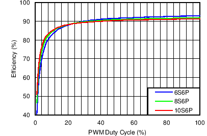
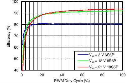
Table 1. Table of Graphs
| TITLE | DESCRIPTION | FIGURE |
|---|---|---|
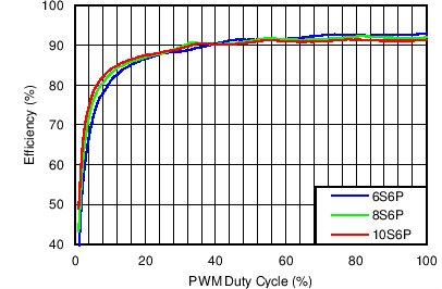
| Efficiency vs PWM Duty in PWM Mode | VIN = 12 V, VOUT = 6S6P, 8S6P, 10S6P, ICS = 20 mA, L = 10 µH | Figure 1 |
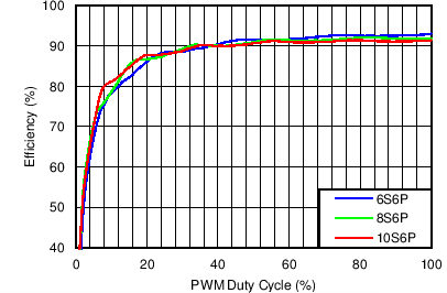
| Efficiency vs PWM Duty in PWM Mode | VIN = 3 V, 12 V, 21 V, VOUT = 6S6P, 8S6P, 10S6P, L = 10 µH | Figure 2 |
| Efficiency vs PWM duty in Mixed Mode | VIN = 12 V, VOUT = 6S6P, 8S6P, 10S6P, ICS = 20 mA, L = 10 µH | Figure 3 |
| Efficiency vs PWM duty in Mixed Mode | VIN = 3 V, 12 V, 21 V, VOUT = 6S6P, 8S6P, 10S6P, L = 10 µH | Figure 4 |
| Efficiency vs PWM duty in Analog Mode | VIN = 12 V, VOUT = 6S6P, 8S6P, 10S6P, ICS = 20 mA, L = 10 µH | Figure 5 |
| Efficiency vs PWM duty in Analog Mode | VIN = 3 V, 12 V, 21 V, VOUT = 6S6P, 8S6P, 10S6P, L = 10 µH | Figure 6 |
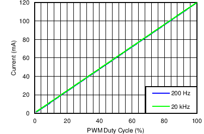
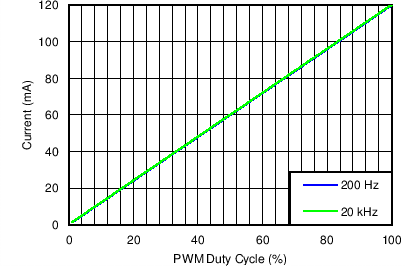
| Dimming Linearity in PWM Mode | VIN = 12 V, VOUT = 10S6P , FDIM = 200 Hz and 20 kHz, L = 10 µH | Figure 7 |
| Dimming Linearity in Mixed Mode | VIN = 12 V, VOUT = 10S6P , FDIM = 200 Hz and 20 kHz, L = 10 µH | Figure 8 |
| Dimming linearity in Analog Mode | VIN = 12 V, VOUT = 10S6P , FDIM = 200 Hz and 20 kHz, L = 10 µH | Figure 9 |
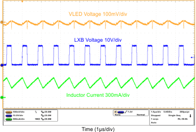
| Switch Waveform | VIN = 3 V, VOUT = 6S6P, Duty = 100%, L = 10 µH | Figure 10 |
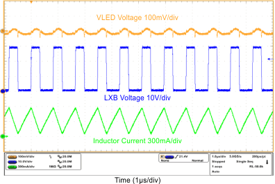
| Switch Waveform | VIN = 12 V, VOUT = 10S6P, Duty = 100%, L = 10 µH | Figure 11 |
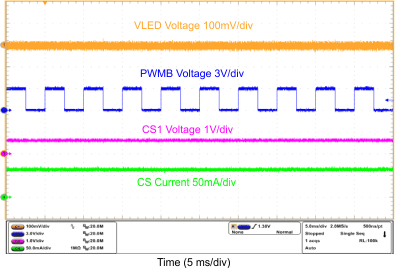
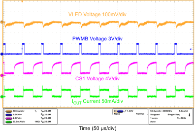
| Mixed-Mode Dimming Ripple | VIN = 12 V, VOUT = 10S6P, FDIM = 200 Hz, Duty = 50%, L = 10 µH | Figure 12 |
| Mixed-Mode Dimming Ripple | VIN = 12 V, VOUT = 10S6P, FDIM = 200 Hz, Duty = 12.5%, L = 10 µH | Figure 13 |
| Mixed-Mode Dimming Ripple | VIN = 12 V, VOUT = 10S6P, FDIM = 20 kHz, Duty = 12.5%, L = 10 µH | Figure 14 |
| PWM-Mode Dimming Ripple | VIN = 12 V, VOUT = 10S6P, FDIM = 200 Hz, Duty = 50%, L = 10 µH | Figure 15 |
| PWM-Mode Dimming Ripple | VIN = 12 V, VOUT = 10S6P, FDIM = 20 kHz, Duty = 50%, L = 10 µH | Figure 16 |

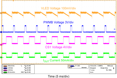
| FDIM = 200 Hz | Duty = 12.5% | |
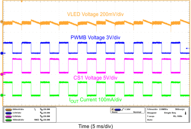
| FDIM = 200 Hz | Duty = 50% | |
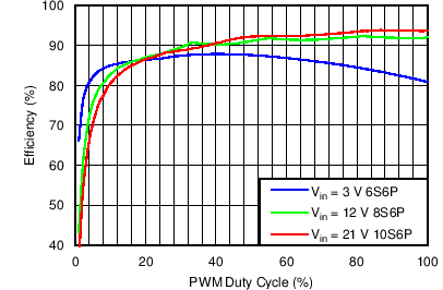
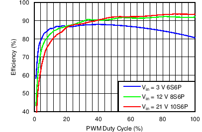
| FDIM = 200 Hz | Duty = 50% | |
| FDIM = 20 kHz | Duty = 12.5% | |
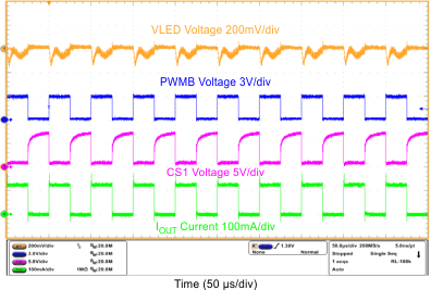
| FDIM = 20 kHz | Duty = 50% | |