SNVSA76B March 2015 – March 2017 TPS61177A
PRODUCTION DATA.
- 1 Features
- 2 Applications
- 3 Description
- 4 Revision History
- 5 Pin Configuration and Functions
- 6 Specifications
-
7 Detailed Description
- 7.1 Overview
- 7.2 Functional Block Diagram
- 7.3
Feature Description
- 7.3.1 Supply Voltage
- 7.3.2 Boost Regulator
- 7.3.3 Programmable Switch Frequency and Slew Rate
- 7.3.4 LED Current Sinks
- 7.3.5 Enable and Start-Up Timing
- 7.3.6 Input Undervoltage Protection (UVLO)
- 7.3.7 Overvoltage Protection (OVP)
- 7.3.8 Current-Sink Open Protection
- 7.3.9 Overcurrent Protection
- 7.3.10 Thermal Protection
- 7.4 Device Functional Modes
- 7.5 Programming
- 7.6
Register Maps
- 7.6.1 MODE (A0h)
- 7.6.2 CS (A1h)
- 7.6.3 UVLO (A2h)
- 7.6.4 FREQ (A3h)
- 7.6.5 SR (A4h)
- 7.6.6 ILIM (A5h)
- 7.6.7 Control (FFh)
- 7.6.8 Example - Writing to a Single RAM Register
- 7.6.9 Example - Writing to Multiple RAM Registers
- 7.6.10 Example - Saving Contents of all RAM Registers to E2PROM
- 7.6.11 Example - Reading from a Single RAM Register
- 7.6.12 Example - Reading from a Single E2PROM Register
- 7.6.13 Example - Reading from Multiple RAM Registers
- 7.6.14 Example - Reading from Multiple E2PROM Registers
- 8 Application and Implementation
- 9 Power Supply Recommendations
- 10Layout
- 11Device and Documentation Support
- 12Mechanical, Packaging, and Orderable Information
Package Options
Mechanical Data (Package|Pins)
- RGR|20
Thermal pad, mechanical data (Package|Pins)
- RGR|20
Orderable Information
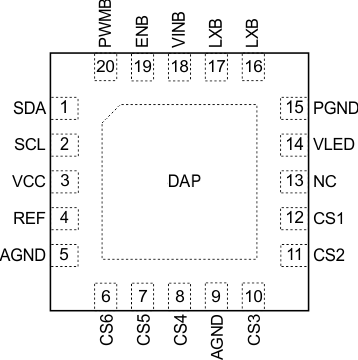
5 Pin Configuration and Functions
RGR Package
20-Pin VQFN
Top View

Pin Functions
| PIN | TYPE | DESCRIPTION | |
|---|---|---|---|
| NAME | NUMBER | ||
| AGND | 5, 9 | — | Signal ground of the device. |
| CS1, CS2, CS3, CS4, CS5, CS6 | 6, 7, 8, 10, 11, 12 | I | Current sink regulation inputs. They are connected to the cathode of WLEDs. The PWM loop regulates the lowest VCS to 500 mV. Each channel is limited to 30-mA current. Connect any unused CS pin to AGND or leave it open. |
| ENB | 19 | I | Enable pin |
| LXB | 16, 17 | I | Drain connection of the internal PWM switch MOSFET and external Schottky diode. |
| REF | 4 | O | The reference pin for internal error amplifier. Connect a 470-nF ceramic capacitor to REF. |
| PGND | 15 | — | Power ground of the IC. Internally, it connects to the source of the PWM switch. Tie the ground of power stage components to this ground. |
| PWMB | 20 | I | Dimming control logic input. The dimming frequency range is from 100 Hz to 25 kHz. |
| SCL | 2 | I | Clock input for I2C interface |
| SDA | 1 | I/O | Data input for I2C interface |
| VCC | 3 | I | Internal pre-regulator and supply rail for the internal logic. Do not connect any capacitor to VCC pin. |
| VINB | 18 | I | Power supply to the IC |
| VLED | 14 | I | The voltage detect pin for VOUT. |