SLVSAN3B December 2010 – November 2016 TPS61199
PRODUCTION DATA.
- 1 Features
- 2 Applications
- 3 Description
- 4 Revision History
- 5 Pin Configuration and Functions
- 6 Specifications
- 7 Detailed Description
- 8 Application and Implementation
- 9 Power Supply Recommendations
- 10Layout
- 11Device and Documentation Support
- 12Mechanical, Packaging, and Orderable Information
Package Options
Mechanical Data (Package|Pins)
Thermal pad, mechanical data (Package|Pins)
- PWP|20
Orderable Information
8 Application and Implementation
NOTE
Information in the following applications sections is not part of the TI component specification, and TI does not warrant its accuracy or completeness. TI’s customers are responsible for determining suitability of components for their purposes. Customers should validate and test their design implementation to confirm system functionality.
8.1 Application Information
The TPS61199 is designed for LCD TV backlighting. It is a current-mode boost controller driving up to eight LED strings in parallel. The input voltage range for the device is from 8 V to 30 V. Its switching frequency is programmed by an external resistor from 300 kHz to 800 kHz.
The TPS61199 has a built-in linear regulator, which steps down the input voltage to the VDD voltage for powering the internal circuitry. An internal soft start circuit is implemented to work with an external capacitor to adjust the soft start-up time to minimize the in-rush current during boost converter start-up.
8.2 Typical Application
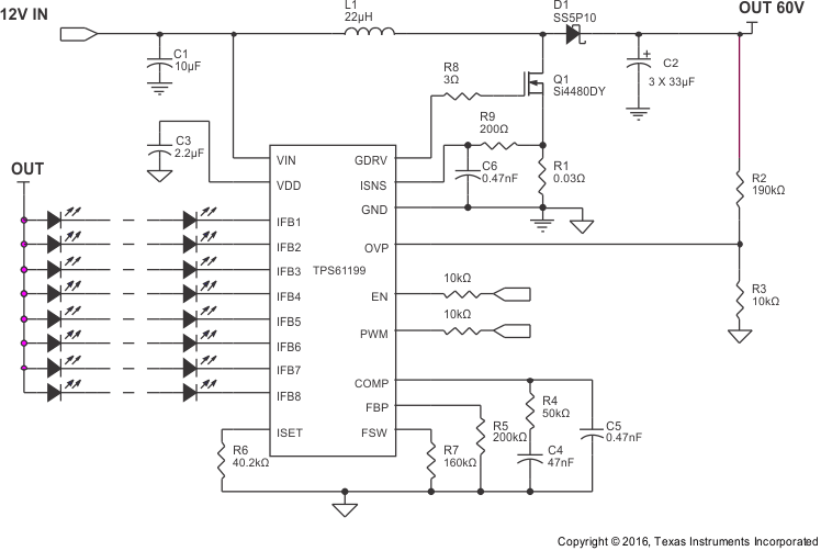
The TPS61199 is configured as a simple boost converter to drive the single string with the LEDs when the boost ratio of the output voltage to the input voltage is less than 6.
 Figure 8. TPS61199 Typical Application
8.2.1 Design Requirements
For typical LED-driver applications, use the parameters listed in Table 2.
Table 2. Design Parameters
| DESIGN PARAMETER | EXAMPLE VALUE |
|---|---|
| Input voltage | 8 V to 30 V |
| Output voltage | 60 V |
| Output current | 60 mA |
| Programmable switching frequency | 300 kHz to 800 kHz |
8.2.2 Detailed Design Procedure
8.2.2.1 Inductor Selection
The TPS61199 is designed to work with inductor values between 10 µH to 47 µH. Running the controller at higher switching frequencies allows the use of smaller and/or lower profile inductors in the 10-µH range. Running the controller at slower switching frequencies requires the use of larger inductors, near 47 µH, to maintain the same inductor current ripple but may improve overall inefficiency due to smaller switching losses. Inductor values can have ±20% tolerance with no current bias. When the inductor current approaches saturation level, its inductance can decrease 20% to 35% from the 0A value depending on how the inductor vendor defines saturation. In a boost regulator, the inductor peak current can be calculated with Equation 6 and Equation 7.


where
- VOUT = output voltage
- IOUT = total LED current
- VIN = input voltage
- η = power conversion efficiency, use 85% for TPS61199 applications
- L = inductor value
- FSW = switching frequency
Select an inductor with a saturation current over the calculated peak current. To calculate the worst case inductor peak current, use the minimum input voltage, maximum output voltage, and maximum total LED current. Select an inductor with a saturation current at least 30% higher the calculated peak current to account for load transients when dimming. Table 3 lists the recommended inductors
Table 3. Recommended Value For Inductors
| DEVICE | L (µH) | DCR (mΩ) | ISAT (A) | SIZE (L × W × H mm) | MANUFACTURER |
|---|---|---|---|---|---|
| CDRH127/HPNP-220M | 22 | 48.8 | 5.6 | 12.5 × 12.5 × 8.0 | Sumida |
| SLF12575T- 220M | 22 | 26.3 | 4 | 12.5 × 12.5 × 7.5 | TDK |
| #B953AS-220M | 22 | 46 | 3.6 | 12.8 × 12.8 × 6.8 | TOKO |
8.2.2.2 Schottky Diode
The TPS61199 demands a high-speed rectification for optimum efficiency. Ensure that the average and peak current ratings of the diode exceed the output LED current and inductor peak current. In addition, the reverse breakdown voltage of the diode must exceed the application output voltage. Therefore, TI recommends the VISHAY SS5P9.
8.2.2.3 Switch MOSFET and Gate Driver Resistor
The TPS61199 demands a power N-MOSFET (see Q1 in Typical Application) as a switch. The voltage and current rating of the MOSFET must be higher than the application output voltage and the inductor peak current. The applications benefits from the addition of a resistor (see R8 in Typical Application) connected between the GDRV pin and the gate of the switching MOSFET. With this resistor, the load regulation between LED dimming on and off period and EMI are improved. TI recommends a 3-Ω resistor value. The TPS61199 exhibits lower efficiency when the resistor value is above 3 Ω.
8.2.2.4 Current Sense and Current Sense Filtering
R1 determines the correct overcurrent limit protection. To choose the right value of R1, start with the total system power needed POUT. Input current Iin = POUT / (VIN × efficiency). Efficinecy can be estimated from Figure 10. The second step is to calculate the inductor ripple current based on the inductor value L.
where
- D = 1 – VIN / VOUT
Thus, the peak current Ipk = Iin + dIL/2. The maximum R1 can now be calculated as
TI recommends adding 20% or more margin to account for component variations.
A small filter placed on the ISNS pin improves performance of the converter (see R9 and C6 in Typical Application). The time constant of this filter should be approximately 100 ns. The range of R9 must be from about 100 Ω to 1 kΩ for best results. Locate C6 as close as possible to the ISNS pin to provide noise immunity.
8.2.2.5 Output Capacitor
The output capacitor is mainly selected to meet the requirements for output ripple and loop stability of the whole system. This ripple voltage is related to the capacitance of the capacitor and its equivalent series resistance (ESR). Assuming a capacitor with zero ESR, the minimum capacitance needed for a given ripple can be calculated by:

where
- Vripplec is the peak to peak output ripple
- DMAX is the duty cycle of the boost converter.
- DMAX is equal to approximately (VOUT_MAX – VIN_MIN) / VOUT_MAX in applications.
Care must be taken when evaluating the derating of a capacitor under DC bias. The DC bias can also significantly reduce capacitance. Ceramic device capacitors can loss as much as 50% of its capacitance at its rated voltage. Therefore, leave the margin on the voltage rating to ensure adequate capacitance in the recommendation table.
The ESR impact on the output ripple must be considered as well if tantalum or electrolytic capacitors are used. Assuming there is enough capacitance such that the ripple due to the capacitance can be ignored, the ESR needed to limit the Vripple is:

Ripple current flowing through the ESR of a capacitor causes power dissipation in the capacitor. This power dissipation causes a temperature increase internal to the capacitor. Excessive temperature can seriously shorten the expected life of a capacitor. Capacitors have ripple current ratings that are dependent on ambient temperature and must not be exceeded. Therefore, three electrolytic capacitors (UPW2A330MPD6, Nichicon) in parallel reduces the total ESR, shown as in Typical Application.
In a typical application, the output requires a capacitor in the range of 10 µF to 100 µF. The output capacitor affects the small signal control loop stability of the boost converter. If the output capacitor is below the range, the boost regulator may potentially become unstable.
8.2.2.6 Loop Consideration
The COMP pin on the TPS61199 is used for external compensation, allowing the loop response to be optimized for each application. The COMP pin is the output of the internal transconductance amplifier. The external resistor R4, along with ceramic capacitors C4 and C5, are connected to the COMP pin to provide poles and zero. The poles and zero, along with the inherent pole and zero in a peak current mode control boost converter, determine the closed loop frequency response. This is important to converter stability and transient response. For most of the applications, the recommended values of 10 kΩ for R4, 100 nF for C4 and 470 pF for C5 are sufficient. For applications with different components or requirements, see Description Compensating the Current Mode Boost Control Loop for guidance on selecting different compensation components.
8.2.3 Application Curves


8.2.4 Additional Application Circuits
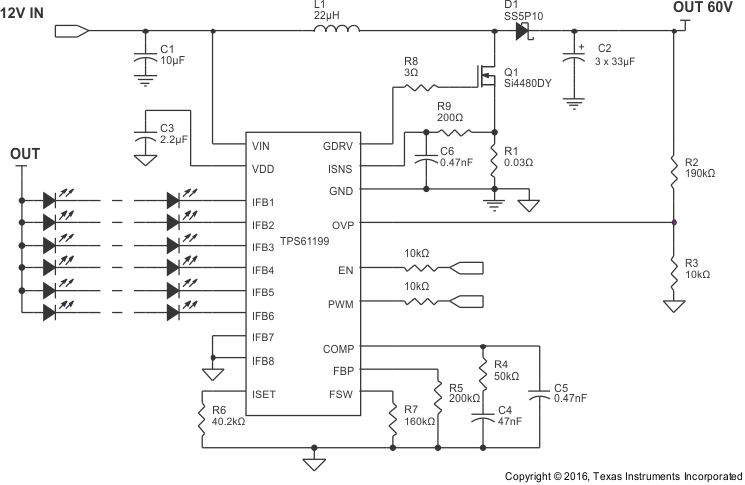
 Figure 11. Six LED Strings Application
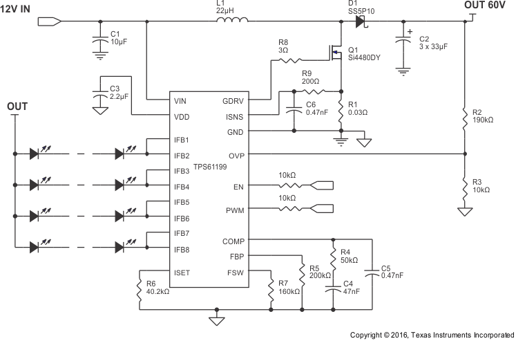
 Figure 12. Four LED Strings With 130-mA Current Application
 Figure 13. 112-LED Driver Application With Ceramic Output Capacitor