SLVSCZ5B
July 2016 – October 2018
TPS61230A
PRODUCTION DATA.
1
Features
2
Applications
3
Description
Device Images
Typical Application
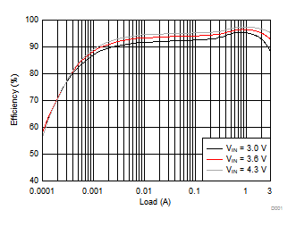
Efficiency
4
Revision History
5
Pin Configuration and Functions
Pin Functions
6
Specifications
6.1
Absolute Maximum Ratings
6.2
ESD Ratings
6.3
Recommended Operating Conditions
6.4
Thermal Information
6.5
Electrical Characteristics
6.6
Typical Characteristics
7
Detailed Description
7.1
Overview
7.2
Functional Block Diagram
7.3
Feature Description
7.3.1
Startup
7.3.2
Enable and Disable
7.3.3
Under-Voltage Lockout (UVLO)
7.3.4
Current Limit Operation
7.3.5
Over Voltage Protection
7.3.6
Load Disconnect
7.3.7
Thermal Shutdown
7.4
Device Functional Modes
7.4.1
PWM Mode
7.4.2
PFM Mode
8
Application and Implementation
8.1
Application Information
8.2
Typical Applications
8.2.1
TPS61230A 2.5-V to 4.5-V Input, 5-V Output Converter
8.2.1.1
TPS61230A 5-V Output Design Requirements
8.2.1.2
TPS61230A 5-V Detailed Design Procedure
8.2.1.2.1
Programming The Output Voltage
8.2.1.2.2
Inductor and Capacitor Selection
8.2.1.2.2.1
Inductor Selection
8.2.1.2.2.2
Output Capacitor Selection
8.2.1.2.2.3
Input Capacitor Selection
8.2.1.2.3
Loop Stability, Feed Forward Capacitor
8.2.1.3
TPS61230A 5-V Output Application Performance Plots
8.2.2
Systems Example - TPS61230A with Feed Forward Capacitor for Best Transient Response
9
Power Supply Recommendations
10
Layout
10.1
Layout Guidelines
10.2
Layout Example
10.3
Thermal Considerations
11
Device and Documentation Support
11.1
Device Support
11.1.1
Third-Party Products Disclaimer
11.2
Documentation Support
11.2.1
Related Documentation
11.3
Receiving Notification of Documentation Updates
11.4
Community Resources
11.5
Trademarks
11.6
Electrostatic Discharge Caution
11.7
Glossary
12
Mechanical, Packaging, and Orderable Information
Package Options
Mechanical Data (Package|Pins)
RNS|7
MPQF449
Thermal pad, mechanical data (Package|Pins)
Orderable Information
slvscz5b_oa
slvscz5b_pm
6.6
Typical Characteristics
V
IN
= 3.6 V, V
OUT
= 5.0 V, T
J
= -40°C to 125 °C, unless otherwise noted.
T
A
= 25 ºC
Figure 1.
Efficiency vs. Output Current
T
A
= 25 ºC
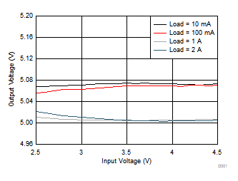
Figure 3.
Line Regulation
T
A
= 25 ºC
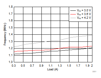
Figure 5.
Frequency vs. Load
V
OUT
= 5 V
V
IN
= 3.6V
Figure 7.
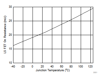
Low-Side FET Rdson vs Junction Temperature
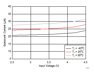
Figure 9.
Quiescent Current vs Input Voltage
Figure 11.
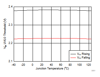
Vin UVLO Threshold vs Junction Temperature
T
A
= 25 ºC
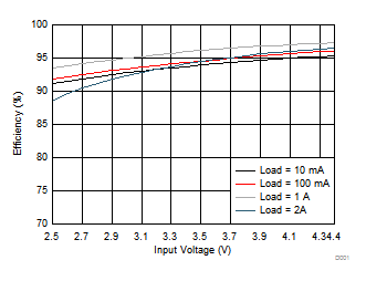
Figure 2.
Efficiency vs. Input Voltage
T
A
= 25 ºC
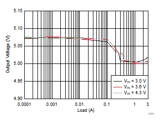
Figure 4.
Load Regulation
V
OUT
= 5 V
V
IN
= 3.6V
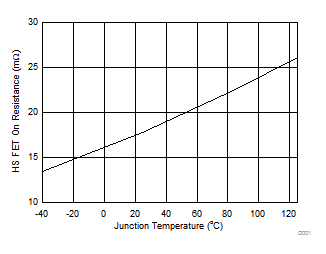
Figure 6.
High-Side FET Rdson vs Junction Temperature
Figure 8.
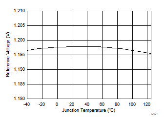
Voltage Reference vs Junction Temperature
Figure 10.
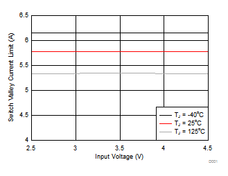
Switch Valley Current Limit vs Input Voltage
Figure 12.
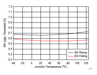
EN logic Threshold vs Junction Temperature