SLVSAO4C December   2010  – June 2020 TPS61240-Q1

PRODUCTION DATA.  

  1. Features
  2. Applications
  3. Description
    1.     Simplified Schematic
  4. Revision History
  5. Pin Configuration and Functions
    1.     Pin Functions
  6. Specifications
    1. 6.1 Absolute Maximum Ratings
    2. 6.2 ESD Ratings
    3. 6.3 Recommended Operating Conditions
    4. 6.4 Thermal Information
    5. 6.5 Electrical Characteristics
    6. 6.6 Typical Characteristics
  7. Detailed Description
    1. 7.1 Overview
    2. 7.2 Functional Block Diagram
    3. 7.3 Feature Description
      1. 7.3.1 Current Limit Operation
      2. 7.3.2 Undervoltage Lockout
      3. 7.3.3 Input Overvoltage Protection
      4. 7.3.4 Enable
      5. 7.3.5 Soft Start
      6. 7.3.6 Load Disconnect
      7. 7.3.7 Thermal Shutdown
    4. 7.4 Device Functional Modes
      1. 7.4.1 Power-Save Mode
  8. Application and Implementation
    1. 8.1 Application Information
    2. 8.2 Typical Applications
      1. 8.2.1 Design Requirements
      2. 8.2.2 Detailed Design Procedure
        1. 8.2.2.1 Programming the Output Voltage
        2. 8.2.2.2 Inductor Selection
        3. 8.2.2.3 Input Capacitor
        4. 8.2.2.4 Output Capacitor
        5. 8.2.2.5 Checking Loop Stability
      3. 8.2.3 Application Curves
    3. 8.3 System Example
  9. Power Supply Recommendations
  10. 10Layout
    1. 10.1 Layout Guidelines
    2. 10.2 Layout Example
  11. 11Device and Documentation Support
    1. 11.1 Documentation Support
      1. 11.1.1 Related Documentation
    2. 11.2 Receiving Notification of Documentation Updates
    3. 11.3 Community Resources
    4. 11.4 Trademarks
    5. 11.5 Electrostatic Discharge Caution
    6. 11.6 Glossary
  12. 12Mechanical, Packaging, and Orderable Information

Package Options

Mechanical Data (Package|Pins)
Thermal pad, mechanical data (Package|Pins)
Orderable Information

Typical Characteristics

Table 1. Table of Graphs

Figure
Maximum output current vs Input voltage Figure 1
Efficiency vs Output current, VOUT = 5 V, VIN = [2.3 V, 3 V, 3.6 V, 4.2 V] Figure 2
vs Input voltage, VOUT = 5 V, IOUT = [100 µA, 1 mA, 10 mA, 100 mA, 200 mA] Figure 3
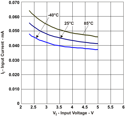
Input current at No output load (PFM Mode) Figure 4
Output voltage vs Output current, VOUT = 5 V, VIN = [2.3 V, 3 V, 3.6 V, 4.2 V] Figure 5
vs Input voltage Figure 6
Frequency vs Output load, VOUT = 5 V, VIN = [3 V, 4 V, 5 V] Figure 7
TPS61240-Q1 io_vi_lvs806.gif
Figure 1. Maximum Output Current vs Input Voltage
TPS61240-Q1 eff_via_lvs806.gif
Figure 3. Efficiency vs Input Voltage for Different Output Current (IO)
TPS61240-Q1 voa_io_lvs806.gif
Figure 5. Output Voltage vs Output Current for Different VIN (VI)
TPS61240-Q1 freqa_io_lvs806.gif
Figure 7. Frequency vs Output Load for Different VIN
TPS61240-Q1 effa_io_lvs806.gif
Figure 2. Efficiency vs Output Current for Different VIN (VI)
TPS61240-Q1 iiq_vi_lvs806.gif
Figure 4. Input Current at No Output Load (PFM Mode) for Different TA
TPS61240-Q1 vo_vi_lvs806.gif
Figure 6. Output Voltage vs Input Voltage for Different Output Current (IO)