-
TPS6125x 3.5-MHz High Efficiency Step-Up Converter In Chip Scale Packaging
- 1 Features
- 2 Applications
- 3 Description
- 4 Revision History
- 5 Device Options
- 6 Pin Configuration and Functions
- 7 Specifications
- 8 Parameter Measurement Information
- 9 Detailed Description
- 10Application and Implementation
- 11Power Supply Recommendations
- 12Layout
- 13Device and Documentation Support
- 14Mechanical, Packaging, and Orderable Information
- IMPORTANT NOTICE
Package Options
Refer to the PDF data sheet for device specific package drawings
Mechanical Data (Package|Pins)
- YFF|9
Thermal pad, mechanical data (Package|Pins)
Orderable Information
TPS6125x 3.5-MHz High Efficiency Step-Up Converter In Chip Scale Packaging
1 Features
- 93% Efficiency at 3.5-MHz Operation
- 21-µA Quiescent Current in Standby Mode
- 37-µA Quiescent Current in Normal Operation
- Wide VIN Range From 2.3 V to 5.5 V
- VIN ≥ VOUT Operation
- IOUT ≥ 800 mA at VOUT = 4.5 V, VIN ≥ 2.65 V
- IOUT ≥ 1000 mA at VOUT = 5.0 V, VIN ≥ 3.3 V
- IOUT ≥ 1500 mA (Peak) at VOUT = 5.0 V, VIN ≥ 3.3 V
- ±2% Total DC Voltage Accuracy
- Light-Load PFM Mode
- Selectable Standby Mode or True Load Disconnect During Shutdown
- Thermal Shutdown and Overload Protection
- Only Three Surface-Mount External Components Required
- Total Solution Size < 25 mm2
- 9-Pin NanoFreeTM (CSP) Packaging
2 Applications
- Cell Phones, Smart Phones
- Mono and Stereo APA Applications
- USB Charging Ports (5V)
3 Description
The TPS6125x device provides a power supply solution for battery-powered portable applications. Intended for low-power applications, the TPS6125x supports up to 800-mA load current from a battery discharged as low as 2.65V and allows the use of low cost chip inductor and capacitors.
With a wide input voltage range of 2.3 V to 5.5 V, the device supports applications powered by Li-Ion batteries with extended voltage range. Different fixed voltage output versions are available from 3.15 V to 5.0 V.
The TPS6125x operates at a regulated 3.5-MHz switching frequency and enters power-save mode operation at light load currents to maintain high efficiency over the entire load current range. The PFM mode extends the battery life by reducing the quiescent current to 37 μA (typ) during light load operation.
In addition, the TPS6125x device can also maintain its output biased at the input voltage level. In this mode, the synchronous rectifier is current limited allowing external load (e.g. audio amplifier) to be powered with a restricted supply. In this mode, the quiescent current is reduced to 21 µA. During shutdown, the load is completely disconnected from the battery. Input current in shutdown mode is less than 1 µA (typ), which maximizes battery life.
The TPS6125x offers a very small solution size due to minimum amount of external components. It allows the use of small inductors and input capacitors to achieve a small solution size.
- For all available packages, see the orderable addendum at the end of the datasheet.
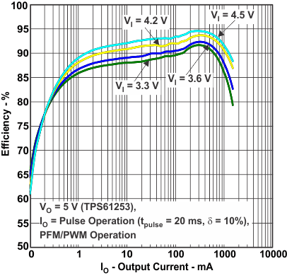
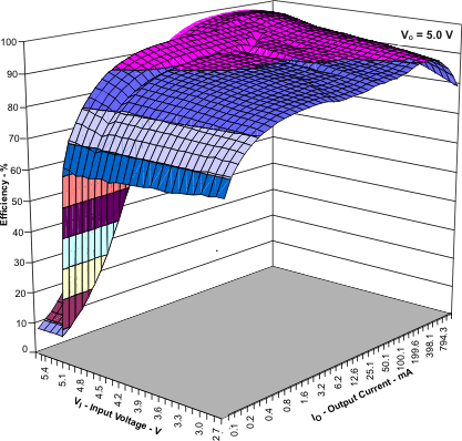
Efficiency vs Load Current
4 Revision History
Changes from F Revision (March 2016) to G Revision
- Changed the Package Dimensions sectionGo
Changes from E Revision (March 2015) to F Revision
- Added device TPS612592Go
Changes from D Revision (December 2014) to E Revision
- Changed Body Size (NOM) from "1.60 mm × 1. 60" to "1.206 mm × 1. 306" in the Device Information table.Go
- Added table note reference to Third-Party Products DisclaimerGo
Changes from C Revision (August 2012) to D Revision
- Added ESD Ratings table, Feature Description section, Device Functional Modes, Application and Implementation section, Power Supply Recommendations section, Layout section, Device and Documentation Support section, and Mechanical, Packaging, and Orderable Information sectionGo
Changes from B Revision (May 2012) to C Revision
- Added TPS61259 to data sheet header as production device.Go
- Changed device TPS61259 to production statusGo
Changes from A Revision (October 2011) to B Revision
- Added TPS61253 and TPS61258 to data sheet header as production devices.Go
- Changed devices TPS61253 and TPS61258 to production statusGo
- Changed graphic entity for Figure 3Go
- Changed graphic entity for Figure 10 and Figure 13Go
- Changed graphic entity for Figure 23Go
Changes from * Revision (September 2011) to A Revision
- Changed device TPS61256 to production statusGo
5 Device Options
| TA | PART NUMBER(1) | OUTPUT VOLTAGE |
DEVICE SPECIFIC FEATURES |
|---|---|---|---|
| –40°C to 85°C | TPS61253 | 5.0 V | Supports 5 V, up to 1500 mA peak loading down to 3.3 V input voltage |
| TPS61254 | 4.5 V | Supports 4.5 V / 800 mA loading down to 2.65 V input voltage |
|
| TPS61255(2) | 3.75 V | ||
| TPS61256 | 5.0 V | Supports 5 V / 900 mA loading down to 3.3 V input voltage |
|
| TPS61257(2) | 4.3 V | ||
| TPS61258 | 4.5 V | Supports 4.5 V, up to 1500 mA peak loading down to 3.3 V input voltage |
|
| TPS61259 | 5.1 V | Supports 5.1 V, up to 1500 mA peak loading down to 3.3 V input voltage |
|
| TPS612592 | 5.2 V | Supports 5.2 V, up to 1500 mA peak loading down to 3.3 V input voltage |
6 Pin Configuration and Functions

Pin Functions
| PIN | I/O | DESCRIPTION | |
|---|---|---|---|
| NAME | NO. | ||
| BP | C3 | I | This is the mode selection pin of the device and is only of relevance when the device is disabled (EN = Low). This pin must not be left floating and must be terminated. Refer to Table 2 for more details. |
| BP = Low: The device is in true shutdown mode. | |||
| BP = High: The output is biased at the input voltage level with a maximum load current capability of ca. 150mA. In standby mode, the device only consumes a standby current of 21µA (typ). | |||
| EN | B3 | I | This is the enable pin of the device. Connecting this pin to ground forces the device into shutdown mode. Pulling this pin high enables the device. This pin must not be left floating and must be terminated. |
| GND | C1, C2 | Ground pin. | |
| SW | B1, B2 | I/O | This is the switch pin of the converter and is connected to the drain of the internal Power MOSFETs. |
| VIN | A3 | I | Power supply input. |
| VOUT | A1, A2 | O | Boost converter output. |
7 Specifications
7.1 Absolute Maximum Ratings
over operating free-air temperature range (unless otherwise noted)(1)| MIN | MAX | UNIT | ||
|---|---|---|---|---|
| Input voltage | Voltage at VIN(2), VOUT(2), SW(2), EN(2), BP(2) | –0.3 | 7 | V |
| Input current | Continuous average current into SW (4) | 1.8 | A | |
| Peak current into SW (5) | 3.5 | |||
| Power dissipation | Internally limited | |||
| Temperature | Operating, TA (3) | –40 | 85 | °C |
| Operating virtual junction, TJ | –40 | 150 | ||
| Storage, Tstg | –65 | 150 | ||
7.2 ESD Ratings
| VALUE | UNIT | |||
|---|---|---|---|---|
| V(ESD) | Electrostatic discharge | Human-body model (HBM), per ANSI/ESDA/JEDEC JS-001(1) | ±2000 | V |
| Charged-device model (CDM), per JEDEC specification JESD22-C101(2) | ±1000 | |||
| Machine model (MM) | ±200 | |||
7.3 Recommended Operating Conditions
| MIN | NOM | MAX | UNIT | |||
|---|---|---|---|---|---|---|
| VI | Input voltage range | TPS61253 | 2.65(1) | 4.85 | V | |
| TPS61254 | 2.5 | 4.35 | ||||
| TPS61256 | 2.5 | 4.85 | ||||
| TPS61257 | 2.5 | 4.15 | ||||
| TPS61258 | 2.65(1) | 4.35 | ||||
| TPS61259 | 2.65(1) | 4.85 | ||||
| TPS612592 | 2.65(1) | 4.85 | ||||
| RL | Minimum resistive load for start-up | TPS6125x | 55 | Ω | ||
| L | Inductance | 0.7 | 1.0 | 2.9 | µH | |
| CO | Output capacitance | 3.5 | 5 | 50 | µF | |
| TA | Ambient temperature | –40 | 85 | °C | ||
| TJ | Operating junction temperature | –40 | 125 | °C | ||
7.4 Thermal Information
| THERMAL METRIC(1) | TPS6125x | UNIT | |
|---|---|---|---|
| YFF | |||
| 9 PINS | |||
| RθJA | Junction-to-ambient thermal resistance | 108.3 | °C/W |
| RθJC(top) | Junction-to-case (top) thermal resistance | 1.0 | |
| RθJB | Junction-to-board thermal resistance | 18 | |
| ψJT | Junction-to-top characterization parameter | 4.2 | |
| ψJB | Junction-to-board characterization parameter | 17.9 | |
7.5 Electrical Characteristics
Minimum and maximum values are at VIN = 2.3V to 5.5V, EN = 1.8V, TA = –40°C to 85°C; Circuit of Parameter Measurement Information section (unless otherwise noted). Typical values are at VIN = 3.6V, EN = 1.8V, TA = 25°C (unless otherwise noted).7.6 Typical Characteristics
Table 1. Table of Graphs
| FIGURE | |||
|---|---|---|---|
| η | Efficiency | vs Output current | Figure 1, Figure 2, Figure 3, Figure 5 |
| vs Input voltage | Figure 4 | ||
| VO | DC output voltage | vs Output current | Figure 6, Figure 7, Figure 8, Figure 9, Figure 10, Figure 14 |
| vs Input voltage | Figure 11 | ||
| IO | Maximum output current | vs Input voltage | Figure 12, Figure 13 |
| ΔVO | Peak-to-peak output ripple voltage | vs Output current | Figure 15, Figure 16, Figure 17 |
| ICC | Supply current | vs Input voltage | Figure 18, Figure 19 |
| ILIM | DC pre-charge current | vs Differential input-output voltage | Figure 20, Figure 21 |
| Valley current limit | vs Temperature | Figure 22, Figure 23 | |
| rDS(on) | MOSFET rDS(on) | vs Temperature | Figure 24 |
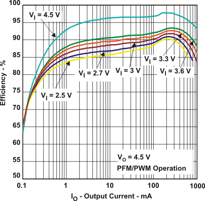 Figure 1. Efficiency vs Output Current
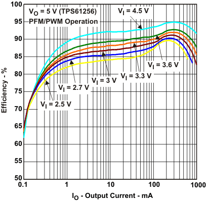 Figure 2. Efficiency vs Output Current
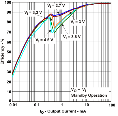 Figure 5. Efficiency vs Output Current
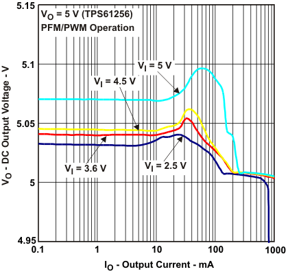 Figure 7. DC Output Voltage vs Output Current
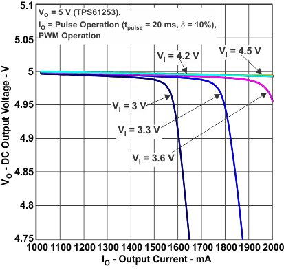
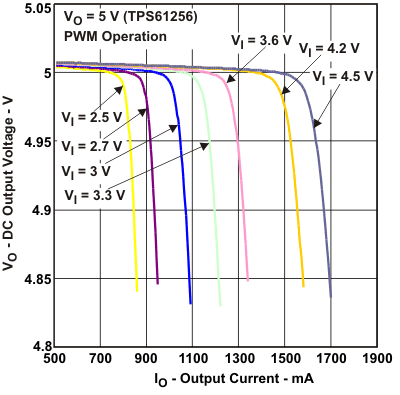 Figure 9. DC Output Voltage vs Output Current
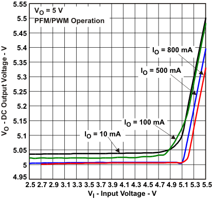 Figure 11. DC Output Voltage vs Input Voltage
 Figure 13. Maximum Output Current vs Input Voltage
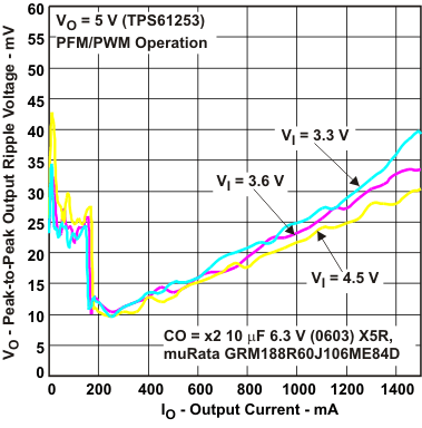
 Figure 15. Peak-to-Peak Output Ripple Voltage vs Output Current
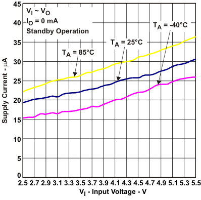 Figure 19. Supply Current vs Input Voltage
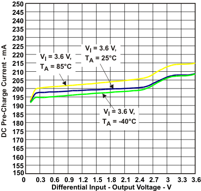 Figure 21. DC Pre-Charge Current vs Differential Input-Output Voltage
 Figure 4. Efficiency vs Input Voltage
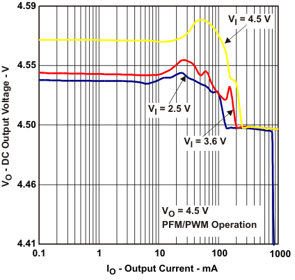 Figure 6. DC Output Voltage vs Output Current
 Figure 8. DC Output Voltage vs Output Current
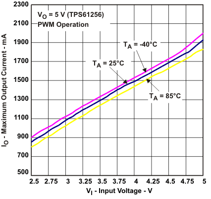 Figure 12. Maximum Output Current vs Input Voltage
 Figure 14. DC Output Voltage vs Output Current
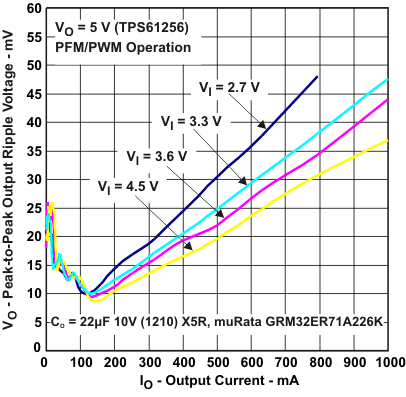 Figure 16. Peak-to-Peak Output Ripple Voltage vs Output Current
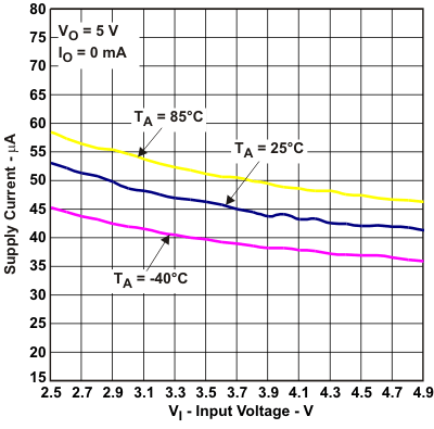 Figure 18. Supply Current vs Input Voltage
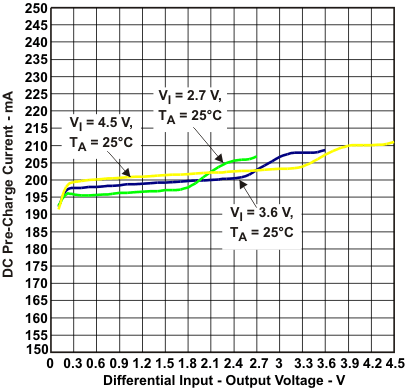 Figure 20. DC Pre-Charge Current vs Differential Input-Output Voltage
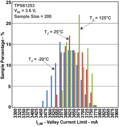
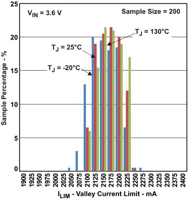 Figure 22. Valley Current Limit
 Figure 24. MOSFET rDS(on) vs Temperature
8 Parameter Measurement Information
 Figure 25. Parameter Measurement Schematic
9 Detailed Description
9.1 Overview
The TPS6125x synchronous step-up converter typically operates at a quasi-constant 3.5-MHz frequency pulse width modulation (PWM) at moderate to heavy load currents. At light load currents, the TPS6125x converter operates in power-save mode with pulse frequency modulation (PFM).
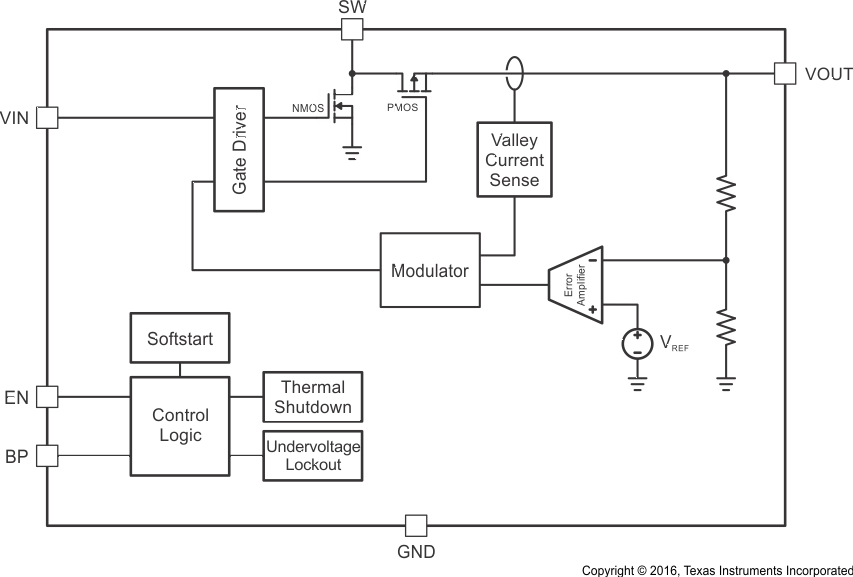
During PWM operation, the converter uses a novel quasi-constant on-time valley current mode control scheme to achieve excellent line/load regulation and allows the use of a small ceramic inductor and capacitors. Based on the VIN/VOUT ratio, a simple circuit predicts the required on-time.
At the beginning of the switching cycle, the low-side N-MOS switch is turned-on and the inductor current ramps up to a peak current that is defined by the on-time and the inductance. In the second phase, once the on-timer has expired, the rectifier is turned-on and the inductor current decays to a preset valley current threshold. Finally, the switching cycle repeats by setting the on timer again and activating the low-side N-MOS switch.
In general, a dc/dc step-up converter can only operate in "true" boost mode, i.e. the output “boosted” by a certain amount above the input voltage. The TPS6125x device operates differently as it can smoothly transition in and out of zero duty cycle operation. Therefore the output can be kept as close as possible to its regulation limits even though the converter is subject to an input voltage that tends to be excessive. In this operation mode, the output current capability of the regulator is limited to ca. 150mA. Refer to Figure 11 for further details.
The current mode architecture with adaptive slope compensation provides excellent transient load response, requiring minimal output filtering. Internal soft-start and loop compensation simplifies the design process while minimizing the number of external components.
9.2 Functional Block Diagram
9.3 Feature Description
9.3.1 Current Limit Operation
The TPS6125x device employs a valley current limit sensing scheme. Current limit detection occurs during the off-time by sensing of the voltage drop across the synchronous rectifier.
The output voltage is reduced as the power stage of the device operates in a constant current mode. The maximum continuous output current (IOUT(CL)), before entering current limit (CL) operation, can be defined by Equation 1.

The duty cycle (D) can be estimated by Equation 2

and the peak-to-peak current ripple (ΔIL) is calculated by Equation 3

The output current, IOUT(DC), is the average of the rectifier ripple current waveform. When the load current is increased such that the lower peak is above the current limit threshold, the off-time is increased to allow the current to decrease to this threshold before the next on-time begins (so called frequency fold-back mechanism). When the current limit is reached the output voltage decreases during further load increase.
Figure 26 illustrates the inductor and rectifier current waveforms during current limit operation.
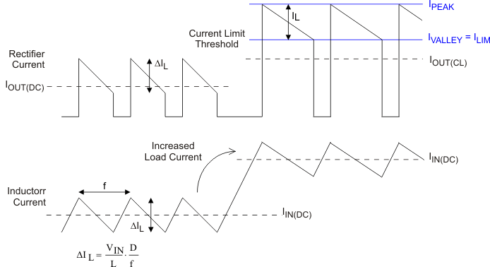 Figure 26. Inductor/Rectifier Currents in Current Limit Operation
9.3.2 Enable
The TPS6125x device starts operation when EN is set high and starts up with the soft-start sequence. For proper operation, the EN pin must be terminated and must not be left floating.
Pulling the EN and BP pins low forces the device in shutdown, with a shutdown current of typically 1 µA. In this mode, true load disconnect between the battery and load prevents current flow from VIN to VOUT, as well as reverse flow from VOUT to VIN.
Pulling the EN pin low and the BP pin high forces the device in standby mode, refer to the Standby Mode section for more details.
9.3.3 Load Disconnect and Reverse Current Protection
Regular boost converters do not disconnect the load from the input supply and therefore a connected battery will be discharged during shutdown. The advantage of TPS6125x is that this converter disconnects the output from the input of the power supply when it is disabled (so called true shutdown mode). In case of a connected battery it prevents it from being discharged during shutdown of the converter.
9.3.4 Softstart
The TPS6125x device has an internal softstart circuit that limits the inrush current during start-up. The first step in the start-up cycle is the pre-charge phase. During pre-charge, the rectifying switch is turned on until the output capacitor is charged to a value close to the input voltage. The rectifying switch is current limited (approximately 200 mA) during this phase. This mechanism is used to limit the output current under short-circuit condition.
Once the output capacitor has been biased to the input voltage, the converter starts switching. The soft-start system progressively increases the on-time as a function of the input-to-output voltage ratio. As soon as the output voltage is reached, the regulation loop takes control and full current operation is permitted.
9.3.5 Undervoltage Lockout
The under voltage lockout circuit prevents the device from malfunctioning at low input voltages and the battery from excessive discharge. It disables the output stage of the converter once the falling VIN trips the under-voltage lockout threshold VUVLO which is typically 2.0V. The device starts operation once the rising VIN trips VUVLO threshold plus its hysteresis of 100 mV at typically 2.1 V.
9.3.6 Thermal Regulation
The TPS6125x device contains a thermal regulation loop that monitors the die temperature during the pre-charge phase. If the die temperature rises to high values of about 110 °C, the device automatically reduces the current to prevent the die temperature from increasing further. Once the die temperature drops about 10 °C below the threshold, the device will automatically increase the current to the target value. This function also reduces the current during a short-circuit condition.
9.3.7 Thermal Shutdown
As soon as the junction temperature, TJ, exceeds 140°C (typ.) the device goes into thermal shutdown. In this mode, the high-side and low-side MOSFETs are turned-off. When the junction temperature falls below the thermal shutdown minus its hysteresis, the device continuous the operation.
9.4 Device Functional Modes
9.4.1 Power Save Mode
The TPS6125x integrates a power save mode to improve efficiency at light load. In power save mode the converter only operates when the output voltage trips below a set threshold voltage.
It ramps up the output voltage with several pulses and goes into power save mode once the output voltage exceeds the set threshold voltage.
The PFM mode is left and PWM mode entered in case the output current can not longer be supported in PFM mode.
 Figure 27. Power Save
9.4.2 Standby Mode
The TPS6125x device is able to maintain its output biased at the input voltage level. In so called standby mode (EN = 0, BP = 1), the synchronous rectifier is current limited to ca. 150mA allowing an external load (e.g. audio amplifier) to be powered with a restricted supply. The output voltage is slightly reduced due to voltage drop across the rectifier MOSFET and the inductor DC resistance. The device consumes only a standby current of 21 µA (typ).
Table 2. Operating Mode Control
| OPERATING MODE | EN | BP |
|---|---|---|
| Shutdown, True Load Disconnect (SD) | 0 | 0 |
| Standby Mode, Output Pre-Biased (SM) | 0 | 1 |
| Boost Operating Mode (BST) | 1 | 0 |
| 1 | 1 |
