SLVSB07A July   2011  – March 2018 TPS61256A

PRODUCTION DATA.  

  1. Features
  2. Applications
  3. Description
    1.     Device Images
      1.      Smallest Solution Size Application
      2.      Efficiency vs. Load Current
  4. Revision History
  5. Pin Configuration and Functions
    1.     Pin Functions
  6. Specifications
    1. 6.1 Absolute Maximum Ratings
    2. 6.2 ESD Ratings
    3. 6.3 Recommended Operating Conditions
    4. 6.4 Thermal Information
    5. 6.5 Electrical Characteristics
    6. 6.6 Typical Characteristics
  7. Parameter Measurement Information
  8. Detailed Description
    1. 8.1 Overview
    2. 8.2 Softstart
    3. 8.3 Undervoltage Lockout
    4. 8.4 Thermal Regulation
    5. 8.5 Thermal Shutdown
    6. 8.6 Functional Block Diagram
    7. 8.7 Feature Description
      1. 8.7.1 Power-Save Mode
      2. 8.7.2 Current Limit Operation
      3. 8.7.3 Enable
      4. 8.7.4 Load Disconnect And Reverse Current Protection
    8. 8.8 Device Functional Modes
      1. 8.8.1 Load Disconnect And Reverse Current Protection
      2. 8.8.2 Softstart
      3. 8.8.3 Undervoltage Lockout
      4. 8.8.4 Thermal Regulation
      5. 8.8.5 Thermal Shutdown
  9. Application and Implementation
    1. 9.1 Application Information
    2. 9.2 Typical Application
      1. 9.2.1 Design Requirements
      2. 9.2.2 Detailed Design Procedure
        1. 9.2.2.1 Inductor Selection
          1. 9.2.2.1.1 High-frequency Converter Applications
        2. 9.2.2.2 Output Capacitor
        3. 9.2.2.3 Input Capacitor
        4. 9.2.2.4 Checking Loop Stability
      3. 9.2.3 Application Curves
  10. 10Power Supply Recommendations
  11. 11Layout
    1. 11.1 Layout Guidelines
    2. 11.2 Layout Example
    3. 11.3 Thermal Information
  12. 12Package Summary
    1. 12.1 Package Dimensions
  13. 13Device and Documentation Support
    1. 13.1 Device Support
      1. 13.1.1 Third-Party Products Disclaimer
    2. 13.2 Receiving Notification of Documentation Updates
    3. 13.3 Community Resources
    4. 13.4 Trademarks
    5. 13.5 Electrostatic Discharge Caution
    6. 13.6 Glossary
  14. 14Mechanical, Packaging, and Orderable Information

Package Options

Mechanical Data (Package|Pins)
Thermal pad, mechanical data (Package|Pins)
Orderable Information

Typical Characteristics

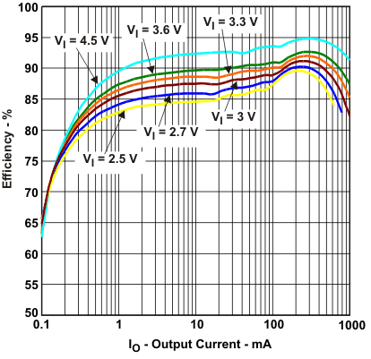
TPS61256A tc3a_lvsag8.gif
Figure 1. Efficiency vs Output Current
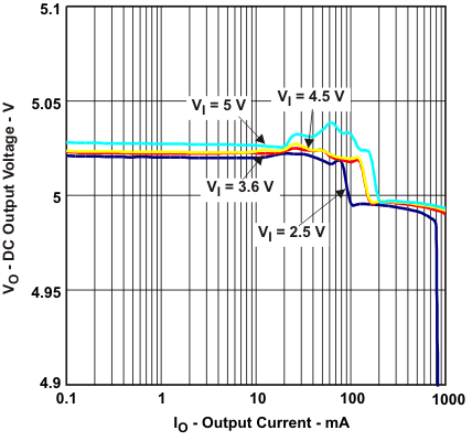
TPS61256A tc5_lvsag8.gif
Figure 3. DC Output Voltage vs Output Current
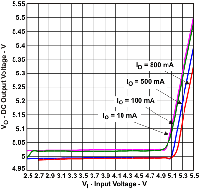
TPS61256A tc7_lvsag8.gif
Figure 5. DC Output Voltage vs Input Voltage
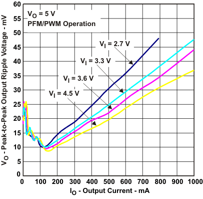
TPS61256A tc9_lvsag8.gif
Figure 7. Peak-To-Peak Output Ripple Voltage vs Output Current
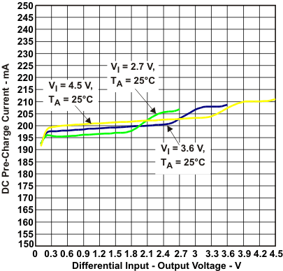
TPS61256A tc11_lvsag8.gif
Figure 9. DC Pre-Charge Currentvs Differential Input-Output Voltage
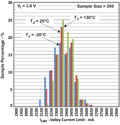
TPS61256A tc13_lvsag8.gif
Figure 11. Valley Current Limit
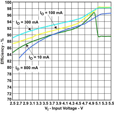
TPS61256A tc4_lvsag8.gif
Figure 2. Efficiency vs Input Voltage
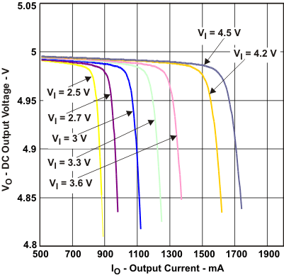
TPS61256A tc6_lvsag8.gif
Figure 4. DC Output Voltage vs Output Current
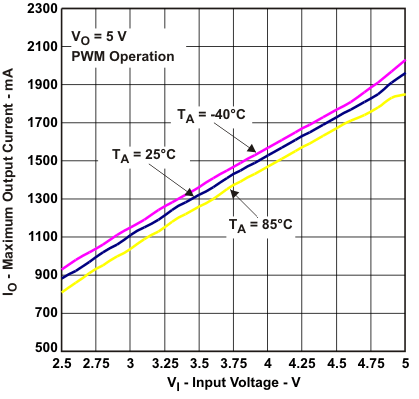
TPS61256A tc8_lvsag8.gif
Figure 6. Maximum Output Currentvs Input Voltage
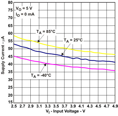
TPS61256A tc10_lvsag8.gif
Figure 8. Supply Currentvs Input Voltage
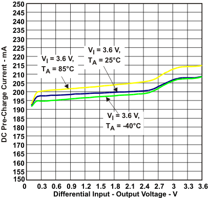
TPS61256A tc12_lvsag8.gif
Figure 10. DC Pre-Charge Currentvs Differential Input-Output Voltage
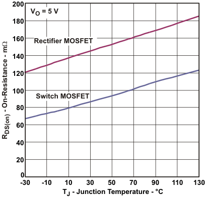
TPS61256A tc14_lvsag8.gif
Figure 12. MOSFET Rds(On) vs Temperature