SLVSEA0B january   2018  – june 2023 TPS61280D , TPS61280E , TPS61281D

PRODUCTION DATA  

  1.   1
  2. Features
  3. Applications
  4. Description
  5. Revision History
  6. Description (continued)
  7. Device Comparison Table
  8. Pin Configuration and Functions
  9. Specifications
    1. 8.1 Absolute Maximum Ratings
    2. 8.2 ESD Ratings
    3. 8.3 Recommended Operating Conditions
    4. 8.4 Thermal Information
    5. 8.5 Electrical Characteristics
    6. 8.6 I2C Interface Timing Characteristics #GUID-BD85FD7C-B9AF-4F5D-9DFF-CD61365A592A/SLVS5401494
    7. 8.7 I2C Timing Diagrams
    8. 8.8 Typical Characteristics
  10. Detailed Description
    1. 9.1 Overview
    2. 9.2 Functional Block Diagram
    3. 9.3 Feature Description
      1. 9.3.1 Voltage Scaling Management (VSEL)
      2. 9.3.2 Spread Spectrum, PWM Frequency Dithering
    4. 9.4 Device Functional Modes
      1. 9.4.1 Power-Save Mode
      2. 9.4.2 Pass-Through Mode
      3. 9.4.3 Mode Selection
      4. 9.4.4 Current Limit Operation
      5. 9.4.5 Start-Up and Shutdown Mode
      6. 9.4.6 Undervoltage Lockout
      7. 9.4.7 Thermal Shutdown
      8. 9.4.8 Fault State and Power-Good
    5. 9.5 Programming
      1. 9.5.1 Serial Interface Description (TPS61280D/E)
      2. 9.5.2 Standard-, Fast-, Fast-Mode Plus Protocol
      3. 9.5.3 HS-Mode Protocol
      4. 9.5.4 TPS6128xD/E I2C Update Sequence
    6. 9.6 Register Maps
      1. 9.6.1  Slave Address Byte
      2. 9.6.2  Register Address Byte
      3. 9.6.3  I2C Registers, E2PROM, Write Protect
      4. 9.6.4  E2PROM Configuration Parameters
      5. 9.6.5  CONFIG Register [reset = 0x01]
      6. 9.6.6  VOUTFLOORSET Register [reset = 0x02]
      7. 9.6.7  VOUTROOFSET Register [reset = 0x03]
      8. 9.6.8  ILIMSET Register [reset = 0x04]
      9. 9.6.9  Status Register [reset = 0x05]
      10. 9.6.10 E2PROMCTRL Register [reset = 0xFF]
  11. 10Application and Implementation
    1. 10.1 Application Information
    2. 10.2 Typical Application
      1. 10.2.1 TPS61281D with 2.5V-4.35 VIN, 1500 mA Output Current (TPS61280D with default I2C Configuration)
        1. 10.2.1.1 Design Requirement
        2. 10.2.1.2 Detailed Design Parameters
          1. 10.2.1.2.1 Inductor Selection
          2. 10.2.1.2.2 Output Capacitor
          3. 10.2.1.2.3 Input Capacitor
          4. 10.2.1.2.4 Checking Loop Stability
        3. 10.2.1.3 Application Performance Curves
      2. 10.2.2 TPS61282D with 2.5V-4.35 VIN, 2000 mA Output Current (TPS61280D with I2C Programmable)
        1. 10.2.2.1 Design Requirements
        2. 10.2.2.2 Detailed Design Procedures
        3. 10.2.2.3 Application Performance Curves
  12. 11Power Supply Recommendations
  13. 12Layout
    1. 12.1 Layout Guidelines
    2. 12.2 Layout Example
    3. 12.3 Thermal Information
  14. 13Device and Documentation Support
    1. 13.1 Device Support
      1. 13.1.1 Third-Party Products Disclaimer
    2. 13.2 Receiving Notification of Documentation Updates
    3. 13.3 Support Resources
    4. 13.4 Trademarks
    5. 13.5 Electrostatic Discharge Caution
    6. 13.6 Glossary
  15. 14Mechanical, Packaging, and Orderable Information
    1. 14.1 Package Summary

Package Options

Mechanical Data (Package|Pins)
Thermal pad, mechanical data (Package|Pins)
Orderable Information

Application Performance Curves

GUID-A638DCEE-3261-454C-9E90-4DF11FDC4D34-low.gif
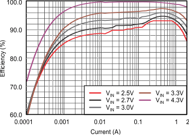
VOUT = 3.3 VVSEL = LowMode = Low
Figure 10-22 TPS61282D Efficiency vs Output Current
GUID-2E8FB0C7-BC7B-4CA9-A56C-FAB8E827FE8E-low.gif
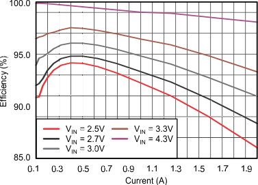
VOUT = 3.5 VVSEL = HighMode = Low
Figure 10-24 TPS61282D Efficiency vs Output Current
GUID-B95A7218-BB81-44B4-A694-A58BBFC3B96B-low.gif
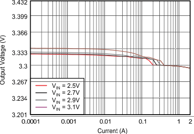
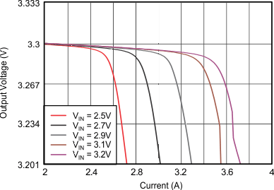
VOUT = 3.3 VMode = Low
Figure 10-26 TPS61282D DC Output Voltage vs Output Current
GUID-AEFE6011-2E33-4F55-9477-43D920DBFEFF-low.gif
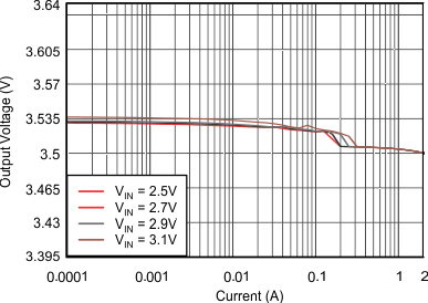
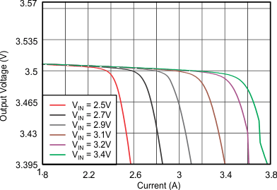
VOUT = 3.5 VMode = Low
Figure 10-28 TPS61282D DC Output Voltage vs Output Current
GUID-857D1175-D444-40E4-9399-5C94CC8F4953-low.gif
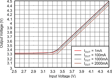
VOUT = 3.3 VVSEL = LowMode = Low
Figure 10-30 TPS61282D DC Output Voltage vs Input Voltage
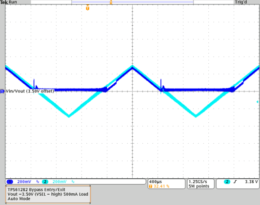
GUID-618FB373-38CA-4C79-BAAA-9DE986789F5A-low.gifFigure 10-32 Boost to Pass-Through Mode Exit / Entry
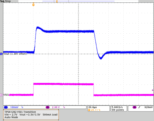
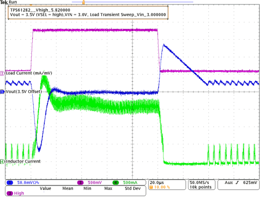
GUID-2CFAC043-085B-4300-A5A5-D4E11156BFF9-low.gifFigure 10-34 TPS61282D Dynamic Voltage Management (VSEL) Load Current 500mA
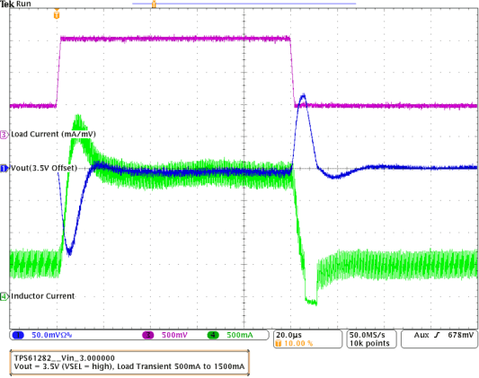
GUID-EFB72FE6-1925-45AE-A02C-3B9243CC6C2D-low.gifFigure 10-36 TPS61282D Load Transient Response In PWM Operation
GUID-65A2FF3A-60FF-4F83-A5D6-60A15596043A-low.gif
VOUT = 3.3 VVSEL = LowMode = Low
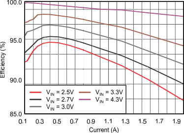
Figure 10-23 TPS61282D Efficiency vs Output Current
GUID-FC3A811D-33CA-417B-9E3E-5915159CF987-low.gif
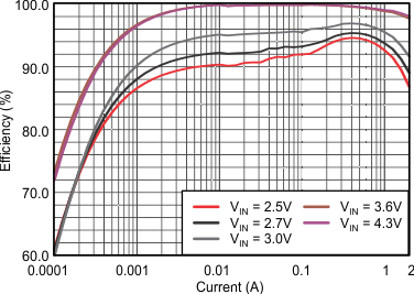
VOUT = 3.5 VVSEL = HighMode = Low
Figure 10-25 TPS61282D Efficiency vs Output Current
GUID-842C39BF-33A5-40EE-95CE-9E3CEF21566D-low.gif
VOUT = 3.3 VMode = Low
Figure 10-27 TPS61282D DC Output Voltage vs Output Current
GUID-4AD11AD8-17EB-410D-A9EA-99816C491AA6-low.gif
VOUT = 3.5 VMode = Low
Figure 10-29 TPS61282D DC Output Voltage vs Output Current
GUID-ACAB0061-7DED-4774-8718-B3CCBCBA0AD6-low.png
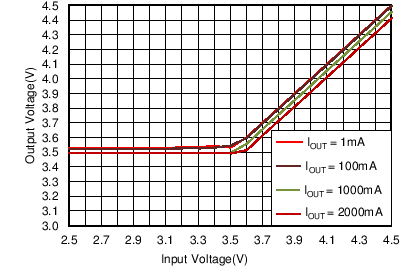
VOUT = 3.5 VVSEL = HighMode = Low
Figure 10-31 TPS61282D DC Output Voltage vs Input Voltage
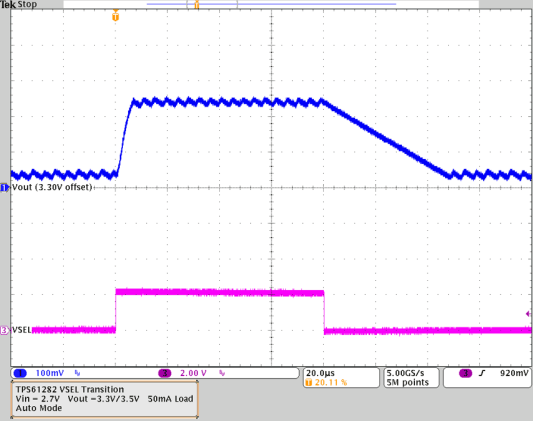
GUID-F36DB426-E4B8-49B5-9300-8D6461F38D88-low.gifFigure 10-33 TPS61282D Dynamic Voltage Management (VSEL) Load Current 50mA
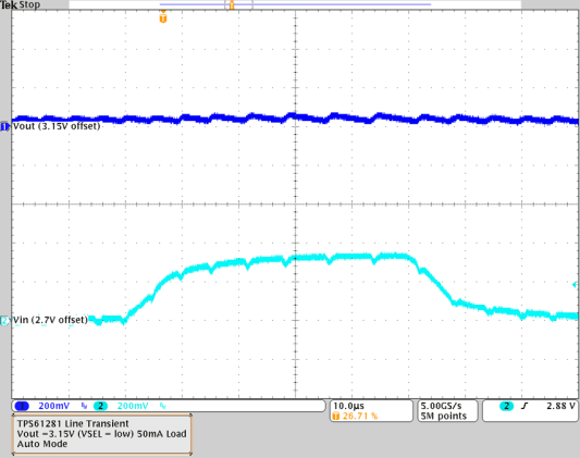
GUID-106560F9-3D52-4E2A-8A06-02E8AB6B5643-low.gifFigure 10-35 TPS61282D Line Transient
GUID-85B3C6E2-44C9-4120-8F96-C0ADA0822528-low.gifFigure 10-37 TPS61282D Load Transient Response In PFM/PWM Operation