SLVSFP3C August 2020 – March 2022 TPS61288
PRODUCTION DATA
- 1 Features
- 2 Applications
- 3 Description
- 4 Revision History
- 5 Device Comparison
- 6 Pin Configuration and Functions
- 7 Specifications
- 8 Detailed Description
- 9 Application and Implementation
- 10Power Supply Recommendations
- 11Layout
- 12Device and Documentation Support
- 13Mechanical, Packaging, and Orderable Information
Package Options
Mechanical Data (Package|Pins)
- RQQ|11
Thermal pad, mechanical data (Package|Pins)
Orderable Information
8.4.2 PFM
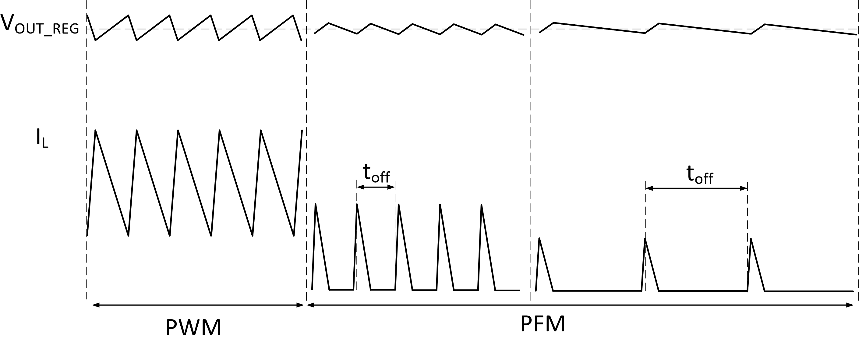
The TPS61288 provides a seamless transition from PWM to PFM operation with smooth on-time/off-time (SOO) mode and enables automatic pulse-skipping mode that provides excellent efficiency over a wide load range. As load current decreasing or VIN rising, the output of the internal error amplifier decreases to lower the inductor peak current, delivering less power to the load. When the output current further decreases, the inductor current will decrease to zero during the off-time. The converter senses inductor current and prevents negative flow by shutting off the high-side MOSFET until the beginning of the next switching cycle.
When the inductor peak current reaches to 2.6 A (typical), along with decreasing peak current, the TPS61288 extends its off-time of the switching period to deliver less energy to the output and regulate the output voltage to the target. The output of the error amplifier continuously goes down and reaches a threshold with respect to the 1.3-A (typical) peak current, the output of the error amplifier is clamped at this value and does not decrease any more.
With SOO mode, the TPS61288 keeps the output voltage equal to the setting voltage. In addition, the output voltage ripple is much smaller at light load due to low peak current. Refer to Figure 8-1. Figure 8-1 PFM Mode
Diagram