SLVS957E June 2009 – April 2016 TPS61300 , TPS61301 , TPS61305
PRODUCTION DATA.
- 1 Features
- 2 Applications
- 3 Description
- 4 Revision History
- 5 Device Comparison Table
- 6 Pin Configuration and Functions
- 7 Specifications
-
8 Detailed Description
- 8.1 Overview
- 8.2 Functional Block Diagrams
- 8.3
Feature Description
- 8.3.1 Safety Timer Accuracy
- 8.3.2 LED Failure Modes and Overvoltage Protection
- 8.3.3 Start-Up Sequence
- 8.3.4 Power Good (Flash Ready)
- 8.3.5 LED Temperature Monitoring (TPS61305, TPS61305A, TPS61306)
- 8.3.6 Hot Die Detector
- 8.3.7 NRESET Input: Hardware Enable and Disable
- 8.3.8 ENDCL Input: DC Light Hardware Control
- 8.3.9 Flashlight Blanking (Tx-MASK)
- 8.3.10 Undervoltage Lockout
- 8.3.11 Storage Capacitor Active Cell Balancing
- 8.3.12 RED Light Privacy Indicator
- 8.3.13 White LED Privacy Indicator
- 8.3.14 Storage Capacitor, Precharge Voltage Calibration
- 8.3.15 Storage Capacitor, Adaptive Precharge Voltage
- 8.3.16 Serial Interface Description
- 8.4
Device Functional Modes
- 8.4.1 Down-Mode in Voltage Regulation Mode
- 8.4.2 LED High-Current Regulators, Unused Inputs
- 8.4.3 Power-Save Mode Operation, Efficiency
- 8.4.4 Mode of Operation: DC Light and Flashlight
- 8.4.5 Flash Strobe is Level Sensitive (STT = 0): LED Strobe Follows FLASH_SYNC Input
- 8.4.6 Flash Strobe Is Leading Edge Sensitive (STT = 1): One-Shot LED Strobe
- 8.4.7 Current Limit Operation
- 8.4.8 Hardware Voltage Mode Selection
- 8.4.9 Shutdown
- 8.4.10 Thermal Shutdown
- 8.4.11 F/S-Mode Protocol
- 8.4.12 HS-Mode Protocol
- 8.4.13 TPS6130xx I2C Update Sequence
- 8.5
Register Maps
- 8.5.1 Slave Address Byte
- 8.5.2 Register Address Byte
- 8.5.3 REGISTER1 (TPS61300, TPS61301)
- 8.5.4 REGISTER1 (TPS61305, TPS61305A, TPS61306)
- 8.5.5 REGISTER2 (TPS61300, TPS61301)
- 8.5.6 REGISTER2 (TPS61305, TPS61305A, TPS61306)
- 8.5.7 REGISTER3
- 8.5.8 REGISTER4
- 8.5.9 REGISTER5
- 8.5.10 REGISTER6 (TPS61300, TPS61301)
- 8.5.11 REGISTER6 (TPS61305, TPS61305A)
- 8.5.12 REGISTER7
-
9 Application and Implementation
- 9.1 Application Information
- 9.2 Typical Applications
- 9.3
System Examples
- 9.3.1 2x 600-mA High-Power White LED Solution Featuring Privacy Indicator
- 9.3.2 White LED Flashlight Driver and Audio Amplifier Power Supply Operating Simultaneously
- 9.3.3 White LED Flashlight Driver and Audio Amplifier Power Supply Operating Simultaneously
- 9.3.4 White LED Flashlight Driver and Audio Amplifier Power Supply Exclusive Operation
- 9.3.5 White LED Flashlight Driver and Auxiliary Lighting Zone Power Supply
- 9.3.6 TPS61300, Typical Application
- 9.3.7 TPS61301, Typical Application
- 9.3.8 TPS61305 Typical Application
- 9.3.9 TPS61306, Typical Application
- 10Power Supply Recommendations
- 11Layout
- 12Device and Documentation Support
- 13Mechanical, Packaging, and Orderable Information
Package Options
Mechanical Data (Package|Pins)
- YFF|20
Thermal pad, mechanical data (Package|Pins)
Orderable Information
8 Detailed Description
8.1 Overview
The TPS6130xx family employs a 2-MHz fixed ON-time, PWM current-mode converter to generate the output voltage required to drive up to three high-power LEDs in parallel. The device integrates a power stage based on an NMOS switch and a synchronous PMOS rectifier. The device also implements a set of linear low-side current regulators to control the LED current when the battery voltage is higher than the diode forward voltage.
A special circuit is applied to disconnect the load from the battery during shutdown of the converter. In conventional synchronous rectifier circuits, the back-gate diode of the high-side PMOS is forward biased in shutdown and allows current flowing from the battery to the output. This device, however, uses a special circuit which takes the cathode of the back-gate diode of the high-side PMOS and disconnects it from the source when the regulator is in shutdown (HC_SEL = L).
The TPS6130xx device cannot only operate as a regulated current source but also as a standard voltage boost regulator featuring power-save mode for improved efficiency at light load. The voltage mode operation can be activated either by a software command or by means of a hardware signal (ENVM). This additional operating mode can be useful to properly synchronize the converter when supplying other high power consuming devices in the system, such as hands-free audio power amplifiers, or any other component requiring a supply voltage higher than the battery voltage.
The TPS6130xx device also supports storage capacitor on its output (so called energy storage mode). In this operating mode (HC_SEL = H), the inductive power stage is used to charge up the super-capacitor to a user-selectable value. Once the charge-up is complete, the LEDs can be fired up to 1025 mA (LED1 and LED3) and 2050 mA (LED2) without causing a battery overload.
In general, a boost converter only regulates output voltages which are higher than the input voltage. This device operates differently. For example, in the voltage mode operation the device is capable of regulating 4.2 V at the output from a battery voltage pulsing as high 5.5 V. To control these applications properly, a down-conversion mode is implemented.
If the input voltage reaches or exceeds the output voltage, the converter changes to a down-conversion mode. In this mode, the control circuit changes the behavior of the rectifying PMOS. It sets the voltage drop across the PMOS as high as needed to regulate the output voltage. This means the power losses in the converter increase. This must be considered for thermal consideration.
In direct drive mode (HC_SEL = L), the power stage is capable of supplying a maximum total current of roughly 1300 to 1500 mA. The TPS61300 provides three constant current inputs, capable of sinking up to 400 mA (LED1 and LED3) and 800 mA (LED2) in flashlight mode.
The TPS6130xx integrates an I2C compatible interface allowing transfers up to 3.4 Mbits/s. This communication interface can be used to set the operating mode (shutdown, constant output current mode vs constant output voltage mode), to control the brightness of the external LED (DC light and flashlight modes), to adjust the output voltage (between 3.825 V and 5.7 V in 125-mV steps) or to program the safety timer for instance. See Register Maps.
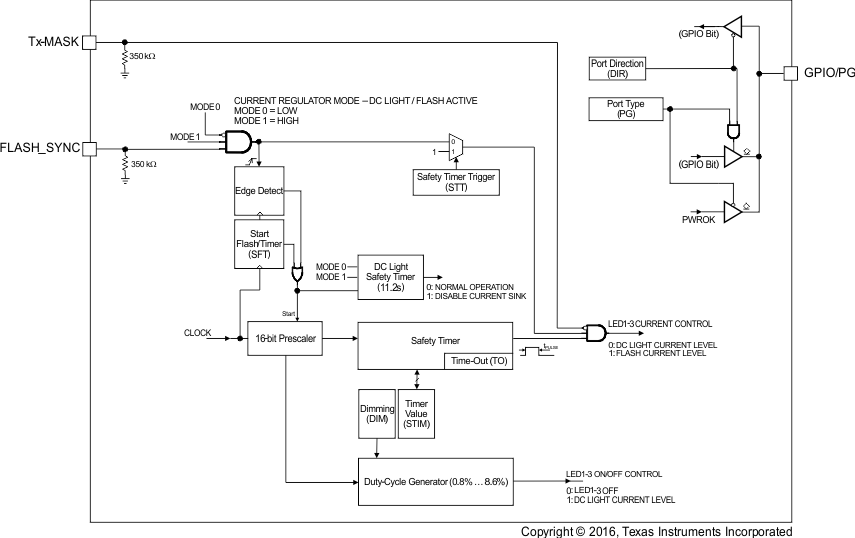
In the TPS6130xx device, the DC light and flash can be controlled either by the I2C interface or by the means of hardware control signals (ENDCL and FLASH_SYNC). To simplify flashlight synchronization with the camera module, the device offers a FLASH_SYNC strobe input pin to turn, with zero latency, the LED current from DC light to flashlight.
The maximum duration of the flashlight pulse can be limited by means of an internal user programmable safety timer (STIM). To avoid the LEDs to be kept accidentally ON in DC light mode by software control, the device implements a 11.2-s watchdog timer.
8.2 Functional Block Diagrams
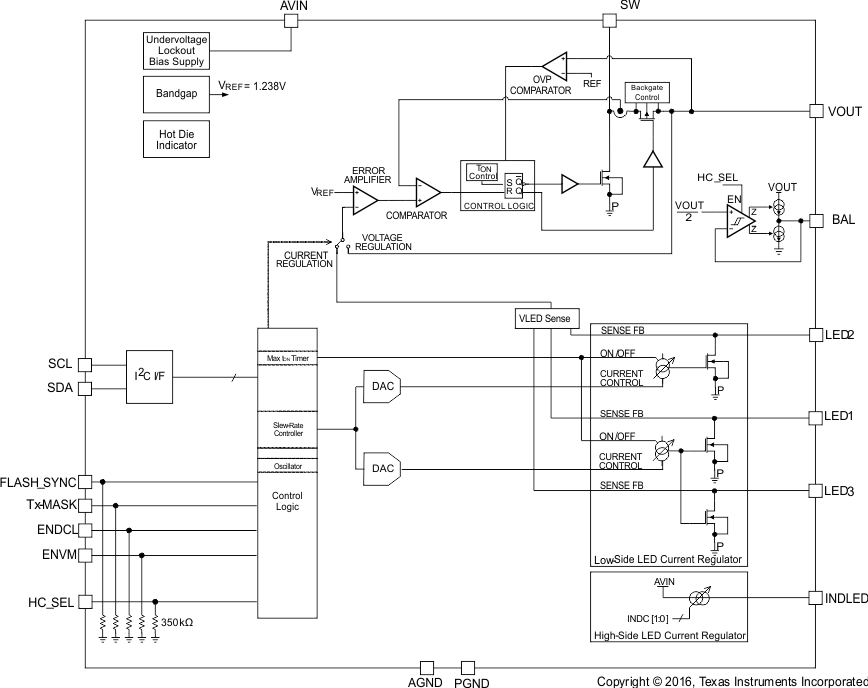
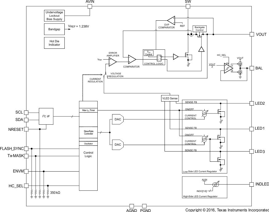
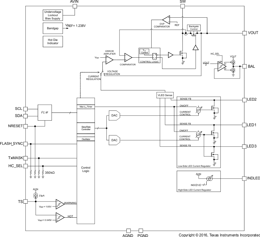
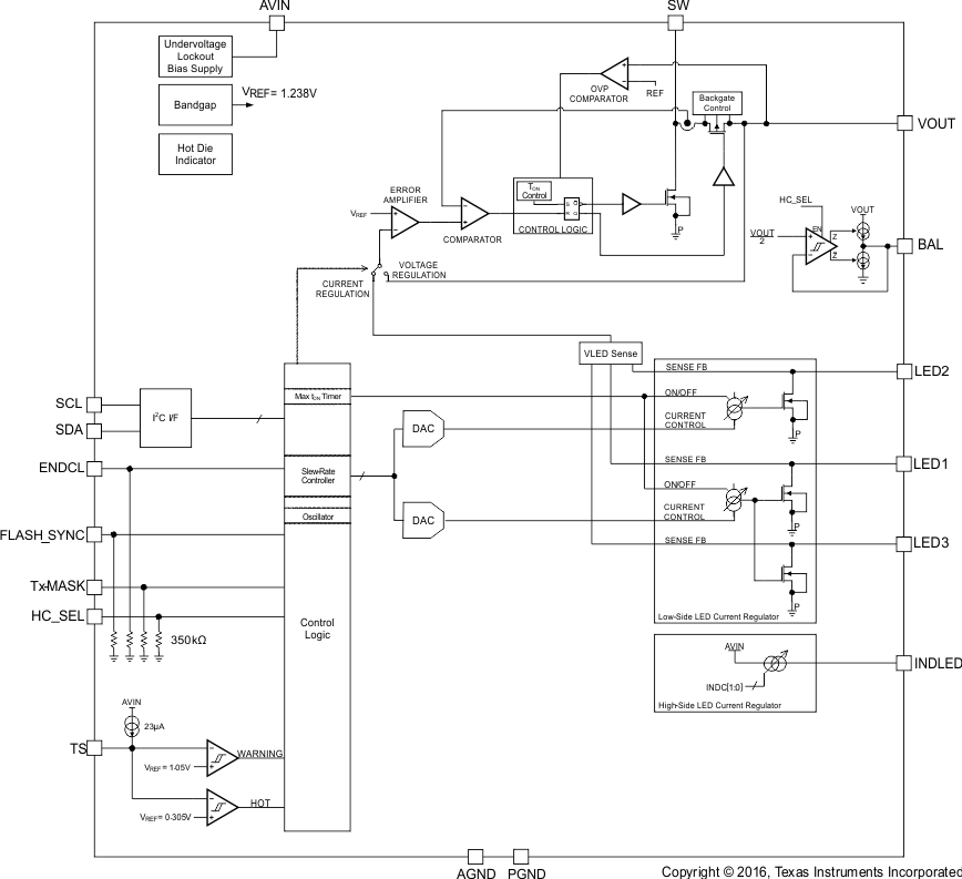
8.3 Feature Description
8.3.1 Safety Timer Accuracy
The LED strobe timer uses the internal oscillator as reference clock. The timer execution speed (see REGISTER3 for more information on STIM[2:0]) scales according to the reference clock accuracy.
Table 3. Frequency for Safety Timer
| OSCILLATOR FREQUENCY | SAFETY TIMER DURATION |
|---|---|
| Minimum | Maximum = Typical × (1 + fACC)(1) |
| Typical | Typical(2) |
| Maximum | Minimum = Typical x (1 – fACC)(1) |
8.3.2 LED Failure Modes and Overvoltage Protection
If a high-power LED fails as a short circuit, the low-side current regulator will limit the maximum output current and the HIGH-POWER LED FAILURE (HPLF) flag will be set.
If a high-power LED fails as an open circuit, the control loop will initially attempt to regulate off of its low-side current regulator feedback signal. This will drive VOUT higher. Because the open-circuited LED will never accept its programmed current, VOUT must be voltage-limited by means of a secondary control loop.
The TPS6130xx device limits VOUT according to the overvoltage protection settings (refer to the OVP specification). In this failure mode, VOUT is either limited to 4.65 V (typical) or 6 V (typical) and the HIGH-POWER LED FAILURE (HPLF) flag is set.
Table 4. Overvoltage Protection Threshold
| OVP THRESHOLD | OPERATING CONDITIONS |
|---|---|
| 4.65-V typical | HC_SEL = L and 0000 ≤ OV[3:0] ≤ 0100 |
| 6-V typical | HC_SEL = H or 0101 ≤ OV[3:0] ≤ 1111 |
See LED High-Current Regulators, Unused Inputs for more information.
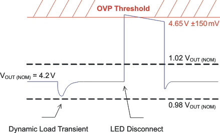 Figure 34. Overvoltage Protection Operation (4.65-V Typical)
8.3.3 Start-Up Sequence
To avoid high inrush current during start-up, take special care to control the inrush current. When the device enables, the internal start-up cycle starts with the first step, the precharge phase.
During precharge, the rectifying switch is turned on until the output capacitor is either charged to a value close to the input voltage or ≈3.3 V, whichever occurs first. The rectifying switch is current-limited during that phase. The current limit increases with decreasing input to output voltage difference. This circuit also limits the output current under short-circuit conditions at the output. Figure 35 shows the typical precharge current vs input minus the output voltage for a specific input voltage.
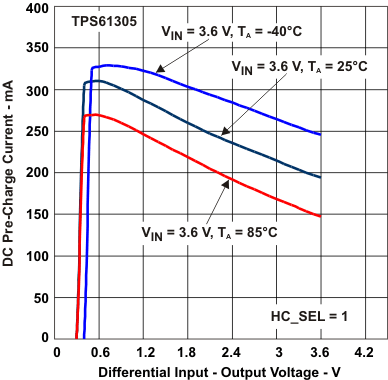 Figure 35. Typical DC Precharge and Short-Circuit Current
In direct drive mode (HC_SEL = L, TPS6130xx), after having precharged the output capacitor, the device starts-up switching and increases its current limit in three steps of typically 250 mA, 500 mA, and full current limit (ILIM setting). The current limit transitions from the first to the second step occurs after a milli-second operation. Full current limit operation is set once the output voltage has reached its regulation limits. In this mode, the active balancing circuit is disabled.
In high-current mode (HC_SEL = H), the precharge voltage of the storage capacitor is depending on the input voltage and operating mode (for example, voltage regulation vs current regulation mode). In case the device is set for exclusive current regulation operation (that is, MODE_CTRL[1:0] = 01 or 10 and ENVM = 0), the output capacitor precharge voltage will be close to the input voltage. Under all other operating conditions, the precharge voltage will either be close to the input voltage or to approximately 3.3 V, whichever is lower.
After having precharged the storage capacitor, the device starts-up switching. During down-mode operation, the inductor valley current is actively limited either to 250 mA or 500 mA (refer to ILIM setting). As the device enters boost mode operation, the current limit transitions to its full capability (refer to ILIM setting and Tx-MASK input logic state). As a consequence, the output voltage ramps up linearly and the start-up time needed to reach the programmed output voltage (see REGISTER6 (TPS61300, TPS61301) or REGISTER6 (TPS61305, TPS61305A) for the OV[3:0] bits) will mainly depend on the super-capacitor value and load current. In this mode, the active balancing circuit is enabled.
8.3.4 Power Good (Flash Ready)
The TPS6130xx integrates a power good circuitry that is activated when the device is operating in voltage regulation mode (MODE_CTRL[1:0] = 11 or ENVM = 1). In shutdown mode (MODE_CTRL[1:0] = 00, ENDCL = 0 and ENVM = 0), the GPIO/PG pin state is defined in Table 5.
Table 5. GPIO Connection
| GPIOTYPE | GPIO/PG SHUTDOWN STATE |
|---|---|
| 0 | Reset/pulled to ground |
| 1 | Open-drain |
Depending on the GPIO/PG output stage type selection (push-pull or open-drain), the polarity of the power-good output signal (PG) can be inverted or not. The power-good software bit and hardware signal polarity is defined in Table 6.
Table 6. GPIO and PG Status
| GPIOTYPE | PG BIT | GPIO/PG OUTPUT PORT | COMMENTS |
|---|---|---|---|
| 0: push-pull output | 0 | 0 | Output is active high signal polarity |
| 1 | 1 | ||
| 1: open-drain output | 0 | Open-drain | Output is active low signal polarity |
| 1 | Low |
The power good signal is valid when the output voltage is within –1.5% and 2.5% of its nominal value. Conversely, it is asserted low when the voltage mode operation gets suspended (MODE_CTRL[1:0] ≠ 11 and ENVM = 0).
 Figure 36. Power Good Operation (DIR = 1, GPIOTYPE = 1)
The TPS6130xx device uses a control architecture that allows recycling of excessive energy that might be stored in the output capacitor. By reversing the operation of the boost power stage, the converter is capable of transferring energy from its output back into the input source. In this case, the power good signal is deasserted whilst the output voltage is decreasing towards its target value. For example the closest fit voltage the converter can support. See Down-Mode in Voltage Regulation Mode for additional information.
8.3.5 LED Temperature Monitoring (TPS61305, TPS61305A, TPS61306)
The TPS61305, TPS61305A, and TPS61306 devices monitor the LED temperature by measuring the voltage between the TS and AGND pins. An internal current source provides the bias (≈24 μA) for a negative-temperature coefficient resistor (NTC), and the TS pin voltage is compared to internal thresholds (1.05 V and 0.345 V) to protect the LEDs against overheating.
The temperature monitoring related blocks are always active in DC light or flashlight modes. In voltage mode operation (MODE_CTRL[1:0] = 11), the device only activates the TS input when the ENTS bit is set to high. In shutdown mode, the LED temperature supervision is disabled and the quiescent current of the device is dramatically reduced.
The LEDWARN and LEDHOT bits reflect the LED temperature. The LEDWARN bit is set when the voltage seen at the TS pin is lower than 1.05 V. This threshold corresponds to an LED warning temperature value, the device operation is still permitted.
While regulating LED current (for example, DC light or flashlight modes), the LEDHOT bit is latched when the voltage seen at the TS pin is lower than 0.345 V. This threshold corresponds to an excessive LED temperature value, the device operation is immediately suspended (MODE_CTRL[1:0] bits are reset and HOTDIE[1:0] bits are set).
8.3.6 Hot Die Detector
The hot die detector monitors the junction temperature but does not shutdown the device. It provides an early warning to the camera engine to avoid excessive power dissipation thus preventing from thermal shutdown during the next high-power flash strobe.
The hot die detector (HOTDIE[1:0] bits) reflects the instantaneous junction temperature and is always enabled excepted when the device is in shutdown mode (MODE_CTRL[1:0] = 00, ENVM = 0 and ENDCL = 0).
8.3.7 NRESET Input: Hardware Enable and Disable
Some devices out of the TPS6130xx family feature a hardware reset pin (NRESET). This reset pin allows the device to be disabled by an external controller without requiring an I2C write command. Under normal operation, the NRESET pin must be held high to prevent an unwanted reset. When the NRESET is driven low, the I2C control interface and all internal control registers are reset to the default states and the part enters shutdown mode.
8.3.8 ENDCL Input: DC Light Hardware Control
Some devices out of the TPS6130xx family feature a dedicated DC light control input (ENDCL). This logic input can be used to turn on the LEDs for DC light operation. This hardware control pin can be useful to control the torch light functionality from a separate engine (for example, base-band). In this mode of operation, the DC light safety timer is not activated.
The ENDCL input is only active when the device is programmed into shutdown (MODE_CTRL[1:0] = 00) or into voltage regulation mode (MODE_CTRL[1:0] = 11 or ENVM = 1) and the indicator control is turned off (INDC[3:0] = 0000). LED1–3 inputs are controlled according to ENLED[3:1] bit settings.
8.3.9 Flashlight Blanking (Tx-MASK)
In direct drive mode (HC_SEL = 0), the Tx-MASK input signal can be used to disable the flashlight operation, for example, during a RF PA transmission pulse. This blanking function turns the LED from flashlight to DC light thereby reducing almost instantaneously the peak current loading from the battery. The Tx-MASK function has no influence on the safety timer duration.
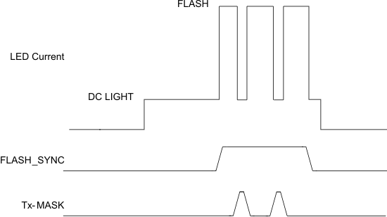 Figure 37. Synchronized Flashlight With Blanking Periods
In high-current mode (HC_SEL = 1), the Tx-MASK input pin is also used to dynamically adjusts the device’s current limit setting which controls the maximum current drawn from the input source. See Current Limit Operation for more information.
8.3.10 Undervoltage Lockout
The undervoltage lockout circuit prevents the device from mis-operation at low input voltages. It prevents the converter from turning on the switch-MOSFET, or rectifier-MOSFET for battery voltages below 2.3 V. The I2C compatible interface is fully functional down to 2.1-V input voltage.
8.3.11 Storage Capacitor Active Cell Balancing
A fully charged super-capacitor will typically have leakage current of under 1 μA. The TPS6130xx device integrates an active balancing feature to cut the total leakage current from the super-capacitor and balance circuit to less than 1.7 μA typically.
The device integrates a window comparator monitoring the tap point of the multi-cell super-capacitor. The balancing output (BAL) is substantially half the actual output voltage (VOUT). If the internal leakage current in one of the capacitors is larger than that in the other, then the voltage at their junction will tend to change in such a way that the voltage on the capacitor with the larger (or largest) leakage current will reduce.
When this happens, a current will begin to flow from the BAL output in such a direction as to reduce the amount by which the voltage changes. The current that will flow after a long period of steady-state conditions will be approximately equal to the difference between the leakage currents of the pair of capacitors which is being balanced by the circuit. The output resistance of the balancing circuit (≈250 Ω) determines how quickly an imbalance will be corrected.
8.3.12 RED Light Privacy Indicator
The TPS6130xx device provides a high-side linear constant current source to drive low VF LEDs. The LED current is directly regulated off the battery and can be controlled through the INDC[3:0] bits. Operation is understood best by referring to the Figure 38 and Figure 39.
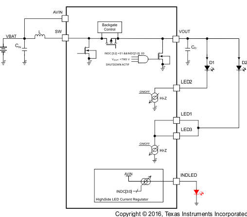 Figure 38. RED Light Indicator, Configuration 1
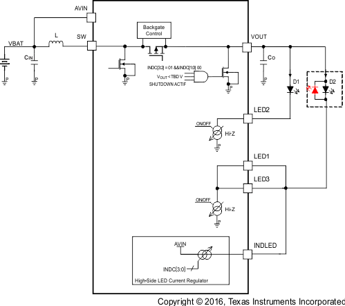 Figure 39. RED Light Indicator, Configuration 2
The device can provide a path to allow for reverse biasing of white LEDs (see Figure 39). To do so, the output of the converter (VOUT) is pulled to ground, thus allowing a reverse current to flow. This mode of operation is only possible when the converter’s power stage is in shutdown (MODE_CTRL[1:0] = 00, ENVM = 0, ENDCL = 0 and HC_SEL = 0).
8.3.13 White LED Privacy Indicator
The TPS6130xx device features white LED drive capability at very low light intensity. To generate a reduced LED average current, the device employs a 122-Hz fixed frequency PWM modulation scheme. Operation is understood best by referring to the timer block diagram.
The DC light current is modulated with a duty cycle defined by the INDC[3:0] bits. The low light dimming mode can only be activated in the software controlled DC light only mode (MODE_CTRL[1:0] = 01, ENVM = X, ENDCL = 0) and applies to the LEDs selected through ENLED[3:1] bits. In this mode, the DC light safety timeout feature is disabled.
 Figure 40. PWM Dimming Principle
8.3.14 Storage Capacitor, Precharge Voltage Calibration
High-power LEDs tend to exhibit a wide forward voltage distribution. The TPS6130xx device integrates a self-calibration procedure that can be used to determine the optimum super-capacitor precharge voltage based on the actual worst case LED forward voltage and ESR of the storage capacitor. This calibration procedure is meant to start-off at a minimum output voltage and can be initiated by setting the SELFCAL bit (preferably with MODE_CTRL[1:0] = 00, ENVM = 0, ENDCL = 0).
The calibration procedure monitors the sense voltage across the low-side current regulators (according to ENLED[3:1] bits setting) and registers the worst case LED (the LED featuring the largest forward voltage). The TPS6130xx device automatically sweeps through its output voltage range and performs a short duration flash strobe for each step (see REGISTER2 (TPS61300, TPS61301) or REGISTER2 (TPS61305, TPS61305A, TPS61306) for FC13[1:0] and FC2[2:0] bits settings).
In direct drive mode (HC_SEL = L), the energy is being directly transferred from the battery to the LEDs. In high-current mode (HC_SEL = H), the energy is supplied exclusively by the output reservoir capacitor and the inductive power stage is turned off for the flash strobe period of time.
The sequence is stopped as soon as the device detects that each of the low-side current regulators have enough headroom voltage (400-mV typical). The device returns the according output voltage in the register OV[3:0] and sets the SELFCAL bit. This bit is only being reset at the or restart of a calibration cycle. In other words, when SELFCAL is asserted the output voltage register (OV[3:0]) returns the result of the last calibration sequence.
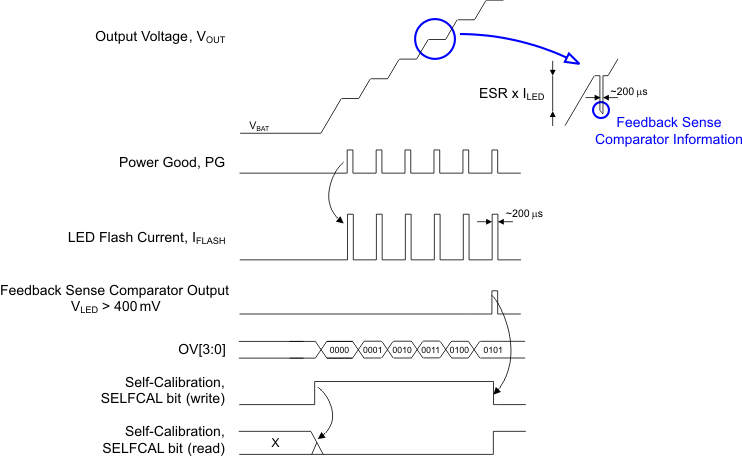 Figure 41. LED Forward Voltage Self-Calibration Principle
8.3.15 Storage Capacitor, Adaptive Precharge Voltage
In high-power LED camera flash applications, the storage capacitor is supposed to be charged to an optimum voltage level in order to:
- Maintain sufficient headroom voltage across the LED current regulators for the entire strobe time.
- Minimize the power dissipation in the device.
High-power LEDs tend to exhibit large dynamic forward voltage variation relating to own self-heating effects. In addition, the energy storage capacitor (Electrochemical Double-Layer Capacitor or Super-Capacitor) also shows a relatively large effective capacitance and ESR spread. The main factors contributing to these variations are:
- Flash strobe duration
- Temperature
- Ageing effects
In practice, it normally becomes very challenging to compensate for all these variations and a worst-case design would presumably be too pessimistic. As a consequence, designers would have to give up the benefits that come with the Storage Capacitor, Precharge Voltage Calibration approach.
The TPS6130xx device offers the possibility of controlling the storage capacitor precharge voltage in a closed-loop manner. The principle is to dynamically adjust the initial prevoltage to the minimum value, as required for the particular components characteristic and operating conditions.
The reference criteria used to evaluate proper operation is the headroom voltage across the LED current regulators. In case of a critical headroom voltage (VLED1-3) at the end of a flash strobe (n cycle), the precharge voltage must be increased before the next capture sequence (n+1 cycle).
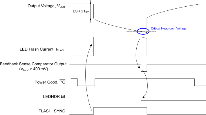 Figure 42. Storage Capacitor, Simple Adaptive Precharge Voltage
8.3.16 Serial Interface Description
I2C is a 2-wire serial interface. The bus consists of a data line (SDA) and a clock line (SCL) with pullup structures. When the bus is idle, both SDA and SCL lines are pulled high. All the I2C compatible devices connect to the I2C bus through open-drain I/O pins, SDA and SCL. A master device, usually a microcontroller or a digital signal processor, controls the bus. The master is responsible for generating the SCL signal and device addresses. The master also generates specific conditions that indicate the START and STOP of data transfer. A slave device receives or transmits data on the bus under control of the master device.
The TPS6130xx device works as a slave and supports the following data transfer modes, as defined in the I2C-Bus Specification: standard mode (100 kbps) and fast mode (400 kbps), and high-speed mode (3.4 Mbps). The interface adds flexibility to the power supply solution, enabling most functions to be programmed to new values depending on the instantaneous application requirements. Register contents remain intact as long as supply voltage remains above 2.1 V.
The data transfer protocol for standard and fast modes is exactly the same, therefore they are referred to as F/S-mode in this document. The protocol for high-speed mode is different from F/S-mode, and it is referred to as HS-mode. The TPS6130xx device supports 7-bit addressing; 10-bit addressing and general call address are not supported. The device 7-bit address is defined as 011 0011.
8.4 Device Functional Modes
8.4.1 Down-Mode in Voltage Regulation Mode
In general, a boost converter only regulates output voltages which are higher than the input voltage. The featured devices come with the ability to regulate 4.2 V at the output with an input voltage being has high as 5.5 V. To control these applications properly, a down-conversion mode is implemented.
In voltage regulation mode, if the input voltage reaches or exceeds the output voltage, the converter changes to the down-conversion mode. In this mode, the control circuit changes the behavior of the rectifying PMOS. It sets the voltage drop across the PMOS as high as needed to regulate the output voltage. This means the power losses in the converter increase. This must be considered for thermal consideration. The down-conversion mode is automatically turned off as soon as the input voltage falls about 200 mV below the output voltage.
For proper operation in down-conversion mode, the output voltage must not be programmed higher than ≈5.3 V. Take care not to violate the absolute maximum ratings at the SW pins.
The TPS6130xx device uses a control architecture that allows to recycle excessive energy that might be stored in the output capacitor. By reversing the operation of the boost power stage, the converter is capable of transferring energy from its output back into the input source.
In high-current mode (HC_SEL = 1), this feature becomes useful to dynamically adjust the output voltage (VOUT) depending on the operating conditions. For example, 4.95-V constant output voltage to support audio applications or variable storage capacitor precharge voltage. See Storage Capacitor, Precharge Voltage Calibration for more information.
Notice that this reverse operating mode can only perform within an output voltage range higher than the input supply. For example, if the storage capacitor is initially precharged to 4.95 V, the input voltage is around 4.1 V and the target output voltage is set to 3.825 V, the converter will only be able to lower the output node down to the input level.
8.4.2 LED High-Current Regulators, Unused Inputs
The TPS6130xx device uses LED forward voltage sensing circuitry on LED1-3 pins to optimize the power stage boost ratio for maximum efficiency. TI recommends not to leave any of the LED1, LED2, or LED3 pins unused if operations has been selected through ENLED[3:1] bits, due to the nature of the sensing circuitry. Leaving LED1-3 pins unconnected, whilst the respective ENLEDx bits have been set, will force the control loop into high gain and eventually trip the output overvoltage protection.
The LED1-3 inputs may be connected together to drive one or two LEDs at higher currents. Connecting the current sink inputs in parallel does not affect the internal operation of the TPS6130xx. For best operation, TI recommends disabling the LED inputs that are not used (see REGISTER5 for ENLED[3:1] bits description).
To achieve smooth LED current waveforms, the TPS61300 device actively controls the LED current ramp-up or down sequence.
Table 7. LED Current Ramp-Up or Down Control vs Operating Mode
| DIRECT DRIVE MODE (HC_SEL = 0) | HIGH-CURRENT MODE (HC_SEL = 1) | |
|---|---|---|
| LED CURRENT RAMP-UP | ISTEP = 25 mA | ISTEP = 56.25 mA |
| tRISE = 12 μs | tRISE = 0.5 μs | |
| Slew-rate ≉ 2.08 mA/μs | Slew-rate ≉ 112.5 mA/μs | |
| LED CURRENT RAMP-DOWN | ISTEP = 25 mA | ISTEP = 56.25 mA |
| tFALL = 0.5 μs | tFALL = 0.5 μs | |
| Slew-rate ≉ 50 mA/μs | Slew-rate ≉ 112.5 mA/μs |
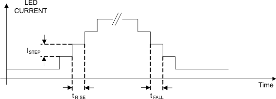 Figure 43. LED Current Slew-Rate Control
In high-current mode (HC_SEL = 1), the LED current settings are defined as a fixed ratio (×2.25) versus the direct drive mode values (HC_SEL = L).
8.4.3 Power-Save Mode Operation, Efficiency
The TPS6130xx device integrates a power save mode to improve efficiency at light load. In power save mode the converter only operates when the output voltage trips below a set threshold voltage. It ramps up the output voltage with one or several pulses and goes again into power save mode once the output voltage exceeds the set threshold voltage.
 Figure 44. Operation in PFM Mode and Transfer to PWM Mode
The power save mode can be enabled and disabled through the ENPSM bit. In down-conversion mode, power save mode is always active and the device cannot be forced into fixed frequency operation at light loads.
The LED sense voltage has a direct effect on the converter’s efficiency. Because the voltage across the low-side current regulator does not contribute to the output power (LED brightness), the lower the sense voltage the higher the efficiency will be.
In direct drive mode (HC_SEL = L), the energy is being directly transferred from the battery to the LEDs. The integrated current control loop automatically selects the minimum boosting ratio to maintain regulation based on the LED forward voltage and current requirements. The low-side current regulators will be dropping the voltage difference between the input voltage and the LEDs forward voltage (VF(LED) < VIN). When running in boost mode (VF(LED) > VIN), the voltage present at the LED1–3 pins of the low-side current regulators will be typically 400 mV leading to high power conversion efficiency. Depending on the input voltage and the LEDs forward voltage characteristic the converter will show efficiency in the range of about 75% to 90%.
In high-current mode (HC_SEL = H), the device is only supplying a limited amount of energy directly from the battery (DC light, contribution to flash current or voltage regulation mode). During a flash strobe, the bulk of the energy supplied to the LEDs is provided by the reservoir capacitor. The low-side current regulators will be typically operating with 400-mV headroom voltage. This means the power losses in the device increase and special care must be taken for thermal considerations.
8.4.4 Mode of Operation: DC Light and Flashlight
Operation is understood best by referring to the timer block diagram. Depending on the settings of MODE_CTRL[1:0] bits the device can enter 4 different operating modes. Table 8 details the converter’s operation for ENVM = 0.
Table 8. Converter Operation for ENVM = 0
| MODE_CTRL[1:0] | DESCRIPTION |
|---|---|
| 00 | The device is in shutdown mode. |
| 01 | The device is regulating the LED current to the DC light current level (DCLC bits) regardless of the FLASH_SYNC input and START_FLASH/TIMER (SFT) bit. To avoid device shutdown by DC light safety timeout, MODE_CTRL[1:0] needs to be refreshed within less than 11.2 s. |
| 10 | The flashlight pulse can be either trigger by a hardware signal (FLASH_SYNC) or by a software bit (SFT). LED strobe pulse follows FLASH_SYNC. |
| 11 | The device is regulating a constant output voltage according to OV[3:0] bits settings. The low-side LED1–3 current sinks are disabled and the LEDs are disconnected from the output. In this operating mode, the safety timer is disabled. |
8.4.5 Flash Strobe is Level Sensitive (STT = 0): LED Strobe Follows FLASH_SYNC Input
FLASH_SYNC and (SFT) = 0: LED operation is set to the DC light current level. To avoid device shutdown by DC light safety timeout, MODE_CTRL[1:0] must be refreshed within less than 11.2 s.
FLASH_SYNC or (SFT) = 1: The LED is driven at the flashlight current level and the safety timer is running. The maximum duration of the flashlight pulse is defined in the STIM[2:0] register.
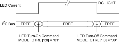 Figure 45. DC Light Operation
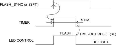 Figure 47. Level Sensitive Safety Timer
(Timeout)
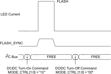 Figure 46. Synchronized Flashlight Strobe
 Figure 48. Level Sensitive Safety Timer
(Normal Operation + Timeout)
The safety timer is started by:
- a rising edge of FLASH_SYNC signal.
- a rising edge of START_FLASH/TIMER (SFT) bit.
The safety timer is stopped by:
- a low level of FLASH_SYNC signal or START_FLASH/TIMER (SFT) bit.
- a timeout signal (TO).
START-FLASH/TIMER (SFT) bit is being reset by the timeout (TO) signal.
8.4.6 Flash Strobe Is Leading Edge Sensitive (STT = 1): One-Shot LED Strobe
When FLASH_SYNC and START_FLASH/TIMER (SFT) are both low the LED operation is set to the DC Light current level. To avoid device shutdown by DC light safety timeout, MODE_CTRL[1:0] needs to be refreshed within less than 11.2 s.
The duration of the flashlight pulse is defined in the STIM register. The flashlight strobe is started by:
- a rising edge of START_FLASH/TIMER (SFT) bit.
- a rising edge of FLASH_SYNC signal.
Once running, the timer ignores all kind of triggering signal and only stops after a timeout (TO). START-FLASH/TIMER (SFT) bit is being reset by the timeout (TO) signal.
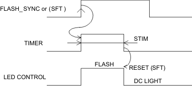 Figure 49. Edge Sensitive Timer
(Single Trigger Event)
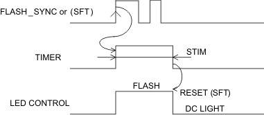 Figure 51. Edge Sensitive Timer
(Multiple Trigger Events)
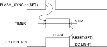 Figure 50. Edge Sensitive Timer
(Single Trigger Event)
8.4.7 Current Limit Operation
The current limit circuit employs a valley current sensing scheme. Current limit detection occurs during the off time through sensing of the voltage drop across the synchronous rectifier. The detection threshold is user selectable through the ILIM bit. The ILIM bit can only be set before the device enters operation (that is, initial shutdown state).
Figure 52 illustrates the inductor and rectifier current waveforms during current limit operation. The output current, IOUT, is the average of the rectifier ripple current waveform. When the load current is increased such that the lower peak is above the current limit threshold, the off time is lengthened to allow the current to decrease to this threshold before the next on-time begins (so called frequency fold-back mechanism).
Both the output voltage and the switching frequency are reduced as the power stage of the device operates in a constant current mode. The maximum continuous output current (IOUT(CL)), before entering current limit operation, can be defined with Equation 1.

The TPS6130xx device also provides a negative current limit (≈300 mA) to prevent an excessive reverse inductor current when the power stage sinks current from the output (that is, storage capacitor) in the forced continuous conduction mode.
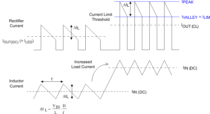 Figure 52. Inductor and Rectifier Currents in Current Limit Operation
To minimize the requirements on the energy storage capacitor present at the output of the driver (HC_SEL = 1), the TPS6130xx device can contribute to a larger extent in supporting directly the high-current LED flash strobe. In fact, the device can dynamically adjust its current limit setting according to the Tx-MASK input.
Table 9. Inductor Current Limit Operation vs HC_SEL and Tx-MASK Inputs
| CURRENT LIMIT SETTING | ILIM BIT | HC_SEL INPUT | Tx-MASK INPUT |
|---|---|---|---|
| 1250 mA | Low | Low | Low |
| 1750 mA | High | Low | Low |
| 1250 mA | Low | High | Low |
| 1750 mA | High | High | Low |
| 1250 mA | Low | Low | High |
| 1750 mA | High | Low | High |
| 250 mA | Low | High | High |
| 500 mA | High | High | High |
8.4.8 Hardware Voltage Mode Selection
The TPS6130xx device integrates a logic input (ENVM) or a software control bit (ENVM bit) that can be used to force the converter to run in voltage mode regulation. Pulling the ENVM pin high forces the device into voltage regulation mode (VOUT is preset to a fixed value, 4.95 V). This additional operating mode can be useful to supply other high power consuming devices in the system, such as hands-free audio power amplifiers, or any other component requiring a regulated supply voltage higher or lower than the battery voltage.
Table 10 gives an overview of the different mode of operation.
Table 10. Operating Mode Description
8.4.9 Shutdown
MODE_CTRL[1:0] bits low force the device into shutdown. The shutdown state can only be entered when the voltage regulation and DC light modes are both turned-off (ENVM = 0 and ENDCL = 0).
In direct drive mode (HC_SEL = L), the regulator stops switching, the high-side PMOS disconnects the load from the input and the LEDx pins are high impedance thus eliminating any DC conduction path. The TPS6130xx device actively discharges the output capacitor when it turns off.
The integrated discharge resistor has a typical resistance of 2 kΩ equally split-off between VOUT to BAL and BAL to GND outputs. The required time to discharge the output capacitor at VOUT depends on load current and the effective output capacitance. The active balancing circuit is disabled and the device consumes only a shutdown current of 1 μA (typical).
In high-current mode (HC_SEL = H), the device maintains its output biased at the input voltage level. In this mode, the synchronous rectifier is current-limited, allowing external load, such as audio amplifiers, to be powered with a restricted supply. The active balancing circuit is enabled and the device consumes only a standby current of 5 μA (typical).
8.4.10 Thermal Shutdown
As soon as the junction temperature, TJ, exceeds 160°C typical, the device goes into thermal shutdown. In this mode, the power stage and the low-side current regulators are turned off, the HOTDIE[1:0] bits are set and can only be reset by a readout.
In the voltage mode operation (MODE_CTRL[1:0] = 11 or ENVM = 1), the device continues its operation when the junction temperature falls below 140°C (typical) again. In the current regulation mode (that is, DC light or flashlight modes) the device operation is suspended.
8.4.11 F/S-Mode Protocol
The master initiates data transfer by generating a start condition. The start condition is when a high-to-low transition occurs on the SDA line while SCL is high, as shown in Figure 53. All I2C-compatible devices will recognize a start condition.
 Figure 53. START and STOP Conditions
The master then generates the SCL pulses, and transmits the 7-bit address and the read/write direction bit R/W on the SDA line. During all transmissions, the master ensures that data is valid. A valid data condition requires the SDA line to be stable during the entire high period of the clock pulse (see Figure 54). All devices recognize the address sent by the master and compare it to their internal fixed addresses. Only the slave device with a matching address generates an acknowledge (see Figure 55) by pulling the SDA line low during the entire high period of the ninth SCL cycle. Upon detecting this acknowledge, the master knows that communication link with a slave has been established.
 Figure 54. Bit Transfer On the Serial Interface
The master generates further SCL cycles to either transmit data to the slave (R/W bit 1) or receive data from the slave (R/W bit 0). In either case, the receiver needs to acknowledge the data sent by the transmitter. So an acknowledge signal can either be generated by the master or by the slave, depending on which one is the receiver. 9-bit valid data sequences consisting of 8-bit data and 1-bit acknowledge can continue as long as necessary.
To signal the end of the data transfer, the master generates a stop condition by pulling the SDA line from low to high while the SCL line is high (see Figure 53). This releases the bus and stops the communication link with the addressed slave. All I2C compatible devices must recognize the stop condition. Upon the receipt of a stop condition, all devices know that the bus is released, and they wait for a start condition followed by a matching address.
Attempting to read data from register addresses not listed in this section will result in 00h being read out.
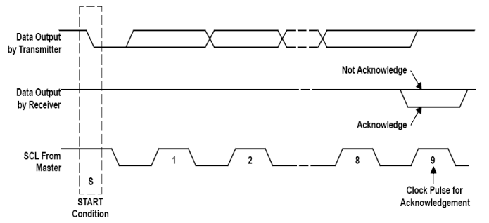 Figure 55. Acknowledge On the I2C Bus
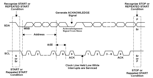 Figure 56. Bus Protocol
8.4.12 HS-Mode Protocol
The master generates a start condition followed by a valid serial byte containing HS master code 00001XXX. This transmission is made in F/S-mode at no more than 400 kbps. No device is allowed to acknowledge the HS master code, but all devices must recognize it and switch their internal setting to support 3.4-Mbps operation.
The master then generates a repeated start condition (a repeated start condition has the same timing as the start condition). After this repeated start condition, the protocol is the same as F/S-mode, except that transmission speeds up to 3.4 Mbps are allowed. A stop condition ends the HS-mode and switches all the internal settings of the slave devices to support the F/S-mode. Instead of using a stop condition, repeated start conditions must be used to secure the bus in HS-mode.
Attempting to read data from register addresses not listed in this section will result in 00h being read out.
8.4.13 TPS6130xx I2C Update Sequence
The TPS6130xx requires a start condition, a valid I2C address, a register address byte, and a data byte for a single update. After the receipt of each byte, TPS6130xx device acknowledges by pulling the SDA line low during the high period of a single clock pulse. A valid I2C address selects the TPS6130xx. TPS6130xx performs an update on the falling edge of the acknowledge signal that follows the LSB byte.
 Figure 57. Write Data Transfer Format in F/S-Mode
 Figure 58. Read Data Transfer Format in F/S-Mode
 Figure 59. Data Transfer Format in HS-Mode
8.5 Register Maps
8.5.1 Slave Address Byte
| MSB | LSB | ||||||
|---|---|---|---|---|---|---|---|
| X | X | X | X | X | X | A1 | A0 |
The slave address byte is the first byte received following the START condition from the master device.
8.5.2 Register Address Byte
| MSB | LSB | ||||||
|---|---|---|---|---|---|---|---|
| 0 | 0 | 0 | 0 | 00 | D2 | D1 | D0 |
Following the successful acknowledgement of the slave address, the bus master will send a byte to the TPS6130xx, which will contain the address of the register to be accessed.
8.5.3 REGISTER1 (TPS61300, TPS61301)
Memory location: 0x01
| 7 | 6 | 5 | 4 | 3 | 2 | 1 | 0 |
| ENVM | MODE_CTRL[1:0] | DCLC13[1:0] | DCLC2[2:0] | ||||
| R/W-0 | R/W-0 | R/W-0 | R/W-0 | R/W-1 | R/W-0 | R/W-0 | R/W-1 |
Table 11. (For example, CONTROL_REVISION Register) Field Descriptions
| Bit | Field | Type | Reset | Description |
|---|---|---|---|---|
| 7 | ENVM | R/W | 0 | Enable Voltage Mode bit.
0: Normal operation. 1: Forces the device into a constant voltage source. In read mode, the ENVM bit is automatically updated to reflect the logic state of the ENVM input pin. |
| 6–5 | MODE_CTRL[1:0] | R/W | 00 | Mode Control bits.
00: Device in shutdown mode. 01: Device operates in DC light mode. 10: Device operates in DC light and flash mode. 11: Device operates as constant voltage source. To avoid device shutdown by DC light safety timeout, MODE_CTRL[1:0] bits need to be refreshed within less than 11.2 s. Writing to REGISTER1[6:5] automatically updates REGISTER2[6:5]. |
| 4–3 | DCLC13[1:0] | R/W | 01 | DC Light Current Control bits (LED1/3).
00: 0 mA. LEDs are off, VOUT set according to OV[3:0].(1)(2) 01: 50 mA 10: 75 mA 11: 100 mA |
| 2–0 | DCLC2[2:0] | R/W | 001 | DC Light Current Control bits (LED2).
000: 0 mA. LEDs are off, VOUT set according to OV[3:0].(1)(2) 001: 50 mA 010: 75 mA 011: 100 mA 100: 125 mA 101: 150 mA 110: 200 mA, 350 mA current level can be activated simultaneously with Tx-MASK = 1. 111: 250 mA, 500 mA current level can be activated simultaneously with Tx-MASK = 1. |
8.5.4 REGISTER1 (TPS61305, TPS61305A, TPS61306)
Memory location: 0x01
| 7 | 6 | 5 | 4 | 3 | 2 | 1 | 0 |
| ENVM | MODE_CTRL[1:0] | DCLC13[1:0] | DCLC2[2:0] | ||||
| R/W-0 | R/W-0 | R/W-0 | R/W-0 | R/W-1 | R/W-0 | R/W-0 | R/W-1 |
Table 12. (For example, CONTROL_REVISION Register) Field Descriptions
| Bit | Field | Type | Reset | Description |
|---|---|---|---|---|
| 7 | ENVM | R/W | 0 | Enable Voltage Mode bit.
0: Normal operation. 1: Forces the device into a constant voltage source. In read mode, the ENVM bit is automatically updated to reflect the logic state of the ENVM input pin. |
| 6–5 | MODE_CTRL[1:0] | R/W | 00 | Mode Control bits.
00: Device in shutdown mode. 01: Device operates in DC light mode. 10: Device operates in DC light and flash mode. 11: Device operates as constant voltage source. To avoid device shutdown by DC light safety timeout, MODE_CTRL[1:0] bits need to be refreshed within less than 11.2 s. Writing to REGISTER1[6:5] automatically updates REGISTER2[6:5]. |
| 4–3 | DCLC13[1:0] | R/W | 01 | DC Light Current Control bits (LED1/3).
00: 0 mA. LEDs are off, VOUT set according to OV[3:0].(1)(2) 01: 55 mA 10: 85 mA 11: 110 mA |
| 2–0 | DCLC2[2:0] | R/W | 001 | DC Light Current Control bits (LED2).
000: 0 mA. LEDs are off, VOUT set according to OV[3:0].(1)(2) 001: 55 mA 010: 85 mA 011: 110 mA 100: 140 mA 101: 165 mA 110: 220 mA, 350 mA current level can be activated simultaneously with Tx-MASK = 1. 111: 275 mA, 500 mA current level can be activated simultaneously with Tx-MASK = 1. |
8.5.5 REGISTER2 (TPS61300, TPS61301)
Memory location: 0x02
| 7 | 6 | 5 | 4 | 3 | 2 | 1 | 0 |
| ENVM | MODE_CTRL[1:0] | FC13[1:0] | FC2[2:0] | ||||
| R/W-0 | R/W-0 | R/W-0 | R/W-0 | R/W-0 | R/W-0 | R/W-1 | R/W-1 |
Table 13. REGISTER2 Field Descriptions
| Bit | Field | Type | Reset | Description | |
|---|---|---|---|---|---|
| 7 | ENVM | R/W | 0 | Enable Voltage Mode bit. 0: Normal operation. 1: Forces the device into a constant voltage source. In read mode, the ENVM bit is automatically updated to reflect the logic state of the ENVM input pin. |
|
| 6–5 | MODE_CTRL[1:0] | R/W | 00 | Mode Control bits.
00: Device in shutdown mode. 01: Device operates in DC light mode. 10: Device operates in DC light and flash mode. 11: Device operates as constant voltage source. To avoid device shutdown by DC light safety timeout, MODE_CTRL[1:0] bits need to be refreshed within less than 11.2 s. Writing to REGISTER2[6:5] automatically updates REGISTER1[6:5]. |
|
| 4–3 | FC13[1:0] | R/W | 00 | Flash Current Control bits (LED1/3).
HC_SEL = 0 000: 275 mA 001: 300 mA 010: 350 mA 011: 450 mA 100: 550 mA 101: 600 mA 110: 700 mA 111: 800 mA |
HC_SEL = 1 000: 650 mA 001: 700 mA 010: 825 mA 011: 1050 mA 100: 1300 mA 101: 1400 mA 110: 1600 mA 111: 1850 mA |
| 2–0 | FC2[2:0] | R/W | 011 | Flash Current Control bits (LED2).
HC_SEL = 0 00: 250 mA 01: 300 mA 10: 350 mA 11: 400 mA |
HC_SEL = 1 00: 600 mA 01: 700 mA 10: 800 mA 11: 925 mA |
8.5.6 REGISTER2 (TPS61305, TPS61305A, TPS61306)
Memory location: 0x02
| 7 | 6 | 5 | 4 | 3 | 2 | 1 | 0 |
| ENVM | MODE_CTRL[1:0] | FC13[1:0] | FC2[2:0] | ||||
| R/W-0 | R/W-0 | R/W-0 | R/W-0 | R/W-0 | R/W-0 | R/W-1 | R/W-1 |
Table 14. REGISTER2 Field Descriptions
| Bit | Field | Type | Reset | Description | |
|---|---|---|---|---|---|
| 7 | ENVM | R/W | 0 | Enable Voltage Mode bit. 0: Normal operation. 1: Forces the device into a constant voltage source. In read mode, the ENVM bit is automatically updated to reflect the logic state of the ENVM input pin. |
|
| 6–5 | MODE_CTRL[1:0] | R/W | 00 | Mode Control bits.
00: Device in shutdown mode. 01: Device operates in DC light mode. 10: Device operates in DC light and flash mode. 11: Device operates as constant voltage source. To avoid device shutdown by DC light safety timeout, MODE_CTRL[1:0] bits need to be refreshed within less than 11.2 s. Writing to REGISTER2[6:5] automatically updates REGISTER1[6:5]. |
|
| 4–3 | FC13[1:0] | R/W | 00 | Flash Current Control bits (LED1/3).
HC_SEL = 0 00: 275 mA 01: 335 mA 10: 385 mA 11: 445 mA |
HC_SEL = 1 00: 665 mA 01: 775 mA 10: 890 mA 11: 1025 mA |
| 2–0 | FC2[2:0] | R/W | 011 | Flash Current Control bits (LED2).
HC_SEL = 0 000: 305 mA 001: 335 mA 010: 385 mA 011: 500 mA 100: 610 mA 101: 665 mA 110: 775 mA 111: 885 mA |
HC_SEL = 1 000: 720 mA 001: 775 mA 010: 915 mA 011: 1165 mA 100: 1450 mA 101: 1550 mA 110: 1775 mA 111: 2050 mA |
8.5.7 REGISTER3
Memory location: 0x03
| 7 | 6 | 5 | 4 | 3 | 2 | 1 | 0 |
| STIM[2:0] | HPLF | SELSTIM (W) TO (R) |
STT | SFT | Tx-MASK | ||
| R/W-1 | R/W-1 | R/W-0 | R-0 | R-0 | R/W-0 | R/W-0 | R/W-1 |
Table 15. REGISTER3 Field Descriptions
| Bit | Field | Type | Reset | Description |
|---|---|---|---|---|
| 7–5 | STIM[2:0] | R/W | 110 | Safety Timer bits
STIM[2:0]: Range 0, Range 1 000: 68.2 ms, 5.3 ms 001: 102.2 ms, 10.7 ms 010: 136.3 ms, 16.0 ms 011: 170.4 ms, 21.3 ms 100: 204.5 ms, 26.6 ms 101: 340.8 ms, 32.0 ms 110: 579.3 ms, 37.3 ms 111: 852 ms, 207.7 ms |
| 4 | HPFL | R | 0 | High-Power LED Failure flag.
0: Proper LED operation. 1: LED failed (open or shorted). High-power LED failure flag is reset after readout |
| 3 | SELSTIM | R | 0 | Safety Timer Selection Range (Write Only).
0: Safety timer range 0. 1: Safety timer range 1. |
| TO | W | Time-Out Flag (Read Only).
0: No time-out event occurred. 1: Time-out event occurred. Time-out flag is reset at re-start of the safety timer. |
||
| 2 | STT | R/W | 0 | Safety Timer Trigger bit.
0: LED safety timer is level sensitive. 1: LED safety timer is rising edge sensitive. This bit is only valid for MODE_CTRL[1:0] = 10. |
| 1 | SFT | R/W | 0 | Start/Flash Timer bit.
In write mode, this bit initiates a flash strobe sequence. 0: No change in the high-power LED current. 1: High-power LED current ramps to the flash current level. In read mode, this bit indicates the high-power LED status. 0: High-power LEDs are idle. 1: Ongoing high-power LED flash strobe. |
| 0 | Tx-MASK | R/W | 1 | Flash Blanking Control bit.
In write mode, this bit enables and disables the flash blanking and LED current reduction function. 0: Flash blanking disabled. 1: LED current is reduced to DC light level when Tx-MASK input is high. In read mode, this flag indicates whether or not the flashlight masking input has been activated. Tx-MASK flag is reset after readout of the flag. 0: No flash blanking event occurred. 1: Tx-MASK input triggered. |
8.5.8 REGISTER4
Memory location: 0x04
| 7 | 6 | 5 | 4 | 3 | 2 | 1 | 0 |
| PG | HOTDIE[1:0] | ILIM | INC[3:0] | ||||
| R/W-0 | R-0 | R-0 | R/W-0 | R/W-0 | R/W-0 | R/W-0 | R/W-0 |
Table 16. REGISTER4 Field Descriptions
| Bit | Field | Type | Reset | Description | |
|---|---|---|---|---|---|
| 7 | PG | R/W | 0 | Power Good bit.
In write mode, this bit selects the functionality of the GPIO/PG output. 0: PG signal is routed to the GPIO port. 1: GPIO PORT VALUE bit is routed to the GPIO port. In read mode, this bit indicates the output voltage conditions. 0: The converter is not operating within the voltage regulation limits. 1: The output voltage is within its nominal value. |
|
| 6–5 | HOTDIE[1:0] | R | 00 | Instantaneous Die Temperature bits.
00: TJ < 55°C 01:55°C < TJ < 70°C 10: TJ > 70°C 11: Thermal shutdown tripped. Indicator flag is reset after readout. |
|
| 4 | ILIM | R/W | 0 | Inductor Valley Current Limit bit.(1)
Current Limit setting, ILIM-bit setting, HC_SEL input level, Tx-MASK input level 1250 mA, Low, Low, Low 1750 mA, High, Low, Low 1250 mA, Low, High, Low 1750 mA, High, High, Low 1250 mA, Low, Low, High 1750 mA, High, Low, High 250 mA, Low, High, High 500 mA, High, High, High |
|
| 3–0 | INDC[3:0] | R/W | 0000 | Indicator Light Control bits.
INDC[3:0]: Privacy indicator INDLED channel 0000: Privacy indicator turned-off 0001: INDLED current = 2.6 mA 0010: INDLED current = 5.2 mA 0011: INDLED current = 7.9 mA 0100: Privacy indicator turned-off 0101: INDLED current = 2.6 mA(2) 0110: INDLED current = 5.2 mA(2) 0111: INDLED current = 7.9 mA (2) |
INDC[3:0]: Privacy indicator LED1–3 channels(3) 1000: 0.8% PWM dimming ratio 1001: 1.6% PWM dimming ratio 1010: 2.3% PWM dimming ratio 1011: 3.1% PWM dimming ratio 1100: 3.9% PWM dimming ratio 1101: 4.7% PWM dimming ratio 1110: 6.3% PWM dimming ratio 1111: 8.6% PWM dimming ratio |
8.5.9 REGISTER5
Memory location: 0x05
| 7 | 6 | 5 | 4 | 3 | 2 | 1 | 0 |
| SELFCAL | ENPSM | STENDCL (R) DIR (W) |
GPIO | GPIOTYPE | ENLED3 | ENLED2 | ENLED1 |
| R/W-0 | R/W-1 | R/W-1 | R/W-0 | R/W-1 | R/W-0 | R/W-1 | R/W-0 |
Table 17. REGISTER5 Field Descriptions
| Bit | Field | Type | Reset | Description |
|---|---|---|---|---|
| 7 | SELFCAL | R/W | 0 | High-Current LED Forward Voltage Self-Calibration Start bit.
In write mode, this bit enables and disables the output voltage vs LED forward voltage and current self-calibration procedure. 0: Self-calibration disabled. 1: Self-calibration enabled. In read mode, this bit returns the status of the self-calibration procedure. 0: Self-calibration ongoing 1: Self-calibration done Notice that this bit is only being reset at the (re-)start of a calibration cycle. |
| 6 | ENPSM | R/W | 1 | Enable and Disable Power-Save Mode bit.
0: Power-save mode disabled. 1: Power-save mode enabled. |
| 5 | STENDCL | R | 1 | ENDCL Input Status bit (Read Only).
This bit indicates the logic state on the ENDCL state. This bit is only active in TPS61300. |
| DIR | W | GPIO Direction bit.
0: GPIO configured as input. 1: GPIO configured as output. |
||
| 4 | GPIO | R/W | 0 | GPIO Port Value.
This bit contains the GPIO port value. |
| 3 | GPIOTYPE | R/W | 1 | GPIO Port Type.
0: GPIO is configured as push-pull output. 1: GPIO is configured as open-drain output. |
| 2 | ENLED3 | R/W | 0 | Enable and Disable High-Current LED3 bit.
0: LED3 input is disabled. 1: LED3 input is enabled. |
| 1 | ENLED2 | R/W | 1 | Enable and Disable High-Current LED2 bit.
0: LED2 input is disabled. 1: LED2 input is enabled. |
| 0 | ENLED1 | R/W | 0 | Enable and Disable High-Current LED1 bit.
0: LED1 input is disabled. 1: LED1 input is enabled. |
8.5.10 REGISTER6 (TPS61300, TPS61301)
Memory location: 0x06
| 7 | 6 | 5 | 4 | 3 | 2 | 1 | 0 |
| NOT USED | LEDHDR | OV[3:0] | |||||
| R/W-0 | R/W-0 | R/W-0 | R-0 | R/W-1 | R/W-0 | R/W-0 | R/W-1 |
Table 18. REGISTER6 Field Descriptions
| Bit | Field | Type | Reset | Description |
|---|---|---|---|---|
| 4 | LEDHDR | R | 0 | LED High-Current Regulator Headroom Voltage Monitoring bit.
This bit returns the headroom voltage status of the LED high-current regulators. This value is being updated at the end of a flash strobe, before the LED current ramp-down phase. 0: Low headroom voltage. 1: Sufficient headroom voltage. |
| 3–0 | OV[3:0] | R/W | 1001 | Output Voltage Selection bits.
In read mode, these bits return the result of the high-current LED forward voltage self-calibration procedure. In write mode, these bits are used to set the target output voltage (see Down-Mode in Voltage Regulation Mode). In applications requiring dynamic voltage control, care must be take to set the new target code after voltage mode operation has been enabled (MODE_CTRL[1:0] = 11 or ENVM bit = 1). OV[3:0]: Target Output Voltage 0000: 3.825 V 0001: 3.950 V 0010: 4.075 V 0011: 4.200 V 0100: 4.325 V 0101: 4.450 V 0110: 4.575 V 0111: 4.700 V 1000: 4.825 V 1001: 4.950 V 1010: 5.075 V 1011: 5.200 V 1100: 5.325 V 1101: 5.450 V 1110: 5.575 V 1111: 5.700 V |
8.5.11 REGISTER6 (TPS61305, TPS61305A)
Memory location: 0x06
| 7 | 6 | 5 | 4 | 3 | 2 | 1 | 0 |
| ENTS | LEDHOT | LEDWARN | LEDHDR | OV[3:0] | |||
| R/W-0 | R/W-0 | R-0 | R-0 | R/W-1 | R/W-0 | R/W-0 | R/W-1 |
Table 19. REGISTER6 Field Descriptions
| Bit | Field | Type | Reset | Description |
|---|---|---|---|---|
| 7 | ENTS | R/W | 0 | Enable and Disable LED Temperature Monitoring.
0: LED temperature monitoring disabled. 1: LED temperature monitoring enabled |
| 6 | LEDHOT | R/W | 0 | LED Excessive Temperature Flag.
This bit can be reset by writing a logic level zero. 0: TS input voltage > 0.345 V. 1: TS input voltage < 0.345 V. |
| 5 | LEDWARN | R | 0 | LED Temperature Warning Flag (Read Only).
This flag is reset after readout. 0: TS input voltage > 1.05 V. 1: TS input voltage < 1.05 V. |
| 4 | LEDHDR | R | 0 | LED High-Current Regulator Headroom Voltage Monitoring bit.
This bit returns the headroom voltage status of the LED high-current regulators. This value is being updated at the end of a flash strobe, before the LED current ramp-down phase. 0: Low headroom voltage. 1: Sufficient headroom voltage. |
| 3–0 | OV[3:0] | R/W | 1001 | Output Voltage Selection bits.
In read mode, these bits return the result of the high-current LED forward voltage self-calibration procedure. In write mode, these bits are used to set the target output voltage (see Down-Mode in Voltage Regulation Mode). In applications requiring dynamic voltage control, care must be take to set the new target code after voltage mode operation has been enabled (MODE_CTRL[1:0] = 11 or ENVM bit = 1). OV[3:0]: Target output voltage 0000: 3.825 V 0001: 3.950 V 0010: 4.075 V 0011: 4.200 V 0100: 4.325 V 0101: 4.450 V 0110: 4.575 V 0111: 4.700 V 1000: 4.825 V 1001: 4.950 V 1010: 5.075 V 1011: 5.200 V 1100: 5.325 V 1101: 5.450 V 1110: 5.575 V 1111: 5.700 V |
8.5.12 REGISTER7
Memory location: 0x07
| 7 | 6 | 5 | 4 | 3 | 2 | 1 | 0 |
| REVID[2:0] | |||||||
| R/W-0 | R/W-0 | R/W-0 | R/W-0 | R/W-0 | R-1 | R-0 | R-0 |
Table 20. REGISTER7 Field Descriptions
| Bit | Field | Type | Reset | Description |
|---|---|---|---|---|
| 2–0 | REVID[2:0](1) | R | 100 | Silicon Revision ID. |