SLVS978D March 2010 – September 2016 TPS61310 , TPS61311
PRODUCTION DATA.
- 1 Features
- 2 Applications
- 3 Description
- 4 Revision History
- 5 Device Comparison Table
- 6 Pin Configuration and Functions
- 7 Specifications
- 8 Parameter Measurement Information
-
9 Detailed Description
- 9.1 Overview
- 9.2 Functional Block Diagram
- 9.3
Feature Description
- 9.3.1 Privacy Indicator
- 9.3.2
Safe Operation and Protection Features
- 9.3.2.1 LED Temperature Monitoring (Finger-Burn Protection)
- 9.3.2.2 LED Failure Modes (Open and Short Detection) and Overvoltage Protection
- 9.3.2.3 LED Current Ramp-Up and Ramp-Down
- 9.3.2.4 Battery Voltage Droop Monitoring and Protection
- 9.3.2.5 Undervoltage Lockout
- 9.3.2.6 Hot Die Detection and Thermal Shutdown
- 9.3.2.7 Current Limit
- 9.3.2.8 Flash Blanking (Tx-Mask) for Instantaneous Flash Current Reduction
- 9.3.3 Start-Up Sequence
- 9.3.4 NRESET Input: Hardware Enable or Disable
- 9.3.5 Serial Interface Description
- 9.3.6 LED Forward Voltage Calibration
- 9.4 Device Functional Modes
- 9.5 Register Maps
- 10Application and Implementation
- 11Power Supply Recommendations
- 12Layout
- 13Device and Documentation Support
- 14Mechanical, Packaging, and Orderable Information
Package Options
Mechanical Data (Package|Pins)
- YFF|20
Thermal pad, mechanical data (Package|Pins)
Orderable Information
10 Application and Implementation
NOTE
Information in the following applications sections is not part of the TI component specification, and TI does not warrant its accuracy or completeness. TI’s customers are responsible for determining suitability of components for their purposes. Customers should validate and test their design implementation to confirm system functionality.
10.1 Application Information
TPS6131x family is based on a high-efficiency synchronous boost topology, which can drive up to three LEDs in parallel. The power stage is capable of supplying a maximum total current up to 1750 mA for TPS61310 and 2480 mA for TPS61311. The 2-MHz switching frequency allows the use of small and low passive components.
10.2 Typical Applications
10.2.1 2x 600-mA High Power White LED Solution Featuring Privacy Indicator
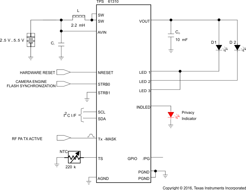 Figure 56. 2x 600-mA High Power White LED Solution Featuring Privacy Indicator
10.2.1.1 Design Requirements
In this design example, different LED current limit is set through I2C interface, the input voltage is 2.5 V to 5.5 V, output voltage is 4.94 V, operating frequency of 2 MHz.
10.2.1.2 Detailed Design Procedure
10.2.1.2.1 Inductor Selection
A boost converter requires two main passive components for storing energy during the conversion. A boost inductor and a storage capacitor at the output are required.
The TPS6131x device integrates current-limit protection circuitry. The valley current of the PMOS rectifier is sensed to limit the maximum current flowing through the synchronous rectifier and the inductor. The valley peak current limit (1250 mA or 1750 mA) is user selectable through the I2C interface.
To optimize solution size the TPS6131x device is designed to operate with inductance values from a minimum of 1.3 µH to a maximum of 2.9 µH. TI recommends a 2.2-µH inductance in typical high-current white LED applications.
The highest peak current through the inductor and the power switch depends on the output load, the input and output voltages. The maximum average inductor current and the maximum inductor peak current can be estimated using Equation 2 and Equation 3:


where
- f = switching frequency (2 MHz)
- L = inductance value (2.2 µH)
- η = estimated efficiency (85%)
The losses in the inductor caused by magnetic hysteresis losses and copper losses are a major parameter for total circuit efficiency.
10.2.1.2.2 Input Capacitor
For good input-voltage filtering, TI recommends low ESR ceramic capacitors. TI recommends a 10-µF input capacitor to improve transient behavior of the regulator and EMI behavior of the total power supply circuit. The input capacitor must be placed as close as possible to the input pin of the converter.
10.2.1.2.3 Output Capacitor
The major parameter necessary to define the output capacitor is the maximum allowed output-voltage ripple of the converter. This ripple is determined by two parameters of the capacitor, the capacitance and the ESR. It is possible to calculate the minimum capacitance required for the defined ripple, supposing that the ESR is zero, by using Equation 4:

where
- f is the switching frequency
- ΔV is the maximum allowed ripple
With a chosen ripple voltage of 10 mV, a minimum capacitance of 10 µF is required. The total ripple is larger due to the ESR of the output capacitor. This additional component of the ripple can be calculated using Equation 5:

The total ripple is the sum of the ripple caused by the capacitance and the ripple caused by the ESR of the capacitor. Additional ripple is caused by load transients. This means that the output capacitor must completely supply the load during the charging phase of the inductor. A reasonable value of the output capacitance depends on the speed of the load transients and the load current during the load change.
For the standard current white LED application, a minimum of 3-µF effective output capacitance is usually required when operating with 2.2-µH (typical) inductors. For solution size reasons, this is usually one or more X5R or X7R ceramic capacitors.
Depending on the material, size and therefore margin to the rated voltage of the used output capacitor, degradation on the effective capacitance can be observed. This loss of capacitance is related to the DC bias voltage applied. Therefore, TI recommends checking that the selected capacitors show enough effective capacitance under real operating conditions.
10.2.1.2.4 NTC Selection
The TPS6131x requires a negative thermistor (NTC) for sensing the LED temperature. Once the temperature monitoring feature is activated, a regulated bias current (approximately 24 µA) is driven out of the TS port to produce a voltage across the thermistor.
If the temperature of the NTC-thermistor rises due to the heat dissipated by the LED, the voltage on the TS input pin decreases. When this voltage goes below the warning threshold, the LEDWARN bit in REGISTER6 is set. This flag is cleared by reading the register.
If the voltage on the TS input decreases further and falls below hot threshold, the LEDHOT bit in REGISTER6 is set and the device goes automatically in shutdown mode to avoid damaging the LED. This status is latched until the LEDHOT flag gets cleared by software.
The selection of the NTC-thermistor value strongly depends on the power dissipated by the LED and all components surrounding the temperature sensor and on the cooling capabilities of each specific application. With a 220-kΩ (at 25°C) thermistor, the valid temperature window is set from 60°C to 90°C. The temperature window can be enlarged by adding external resistors to the TS pin application circuit. To obtain proper triggering of the LEDWARN and LEDHOT flags in noisy environments, the TS signal may require additional filtering capacitance.
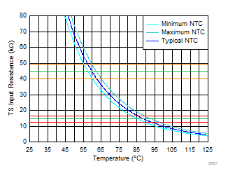 Figure 57. Temperature Monitoring Characteristic
10.2.1.2.5 Checking Loop Stability
The first step of circuit and stability evaluation is to examine these signals from a steady-state perspective:
- Switching node (SW)
- Inductor current (IL)
- Output ripple voltage (VOUT(AC))
These are the basic signals that must be measured when evaluating a switching converter. If the switching waveform shows large duty-cycle jitter or the output voltage or inductor current shows oscillations, the regulation loop may be unstable. This is often a result of improper board layout or L-C combination.
As a next step in the evaluation of the regulation loop, test the load transient response. VOUT can be monitored for settling time, overshoot or ringing that helps judge the converter's stability. With no ringing, the loop usually has more than 45° of phase margin.
Because the damping factor of the circuitry is directly related to several resistive parameters (MOSFET rDS(ON)) that are temperature dependant, the loop stability must be analyzed over the input voltage range, output current range, and temperature range.
10.2.1.2.6 LED Flash Current Level Optimization Versus Battery Droop
In cell phone applications, the camera engine is normally specified over an operating temperature down to 0°C or –10°C. To achieve a reliable system operation, the LED flash current must be rated according to the maximum tolerable battery voltage drop, highest battery impedance and lowest ambient temperature.
To dynamically optimize the LED flash current (light output) versus battery state-of-charge and temperature, we could consider the self-adjustment procedure in Figure 58. This algorithm could be embedded into the auto-exposure, auto white-balance, or red-eye reduction pre-flash algorithms.
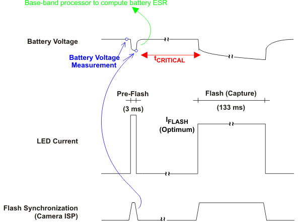 Figure 58. Image Capture Sequence
- Phase 1: Pre-Flash, Battery Impedance Estimation
- Phase 2: Battery Loading Monitoring Before Image Capture
The battery voltage usually drops by a few hundreds of millivolts during a high-power flash strobe. For short durations, this voltage droop should not be subject to the battery intrinsic capacitance (relaxation effect) but rather to its cell impedance.
Based on the state of the Tx-MASK input, the battery voltage drop, during pre-flash, and the LED current level, the base-band processor can compute an estimated cell-impedance value (ESR).
Depending on the ambient temperature, the battery state-of-charge (SoC), the flash (capture) duration and the actual status of the various RF interfaces, the base-band processor can determine a safe battery voltage droop, to be tolerated during the forthcoming strobe sequence, as well as a maximum flash current rating. The maximum flash current setting can be estimated by considering nominal LEDs and approximately 85% power efficiency in the driver.
For a reliable system operation, the base-band processor must make sure that no 'parasitic' high-current load suddenly impacts the budgeted battery voltage sag. The most critical timing is referenced as tCRITICAL.
The interrupt subroutine, running on the base-band processor, must be ready to detect any 'parasitic' battery load event that could occur before the image capture (see REGISTER3 (address = 0x03) for SFT bit description). In such a situation, the battery voltage droop budget and the maximum LED current settings would need to be revised.
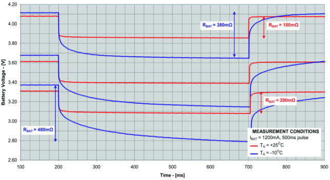 Figure 59. 900-mAh, Li-Ion Battery Transient Response vs SoC and Temperature
10.2.1.3 Application Curves
| STRB1 = 0 |
| STRB1 = 0 |
| STRB1 = 0 |
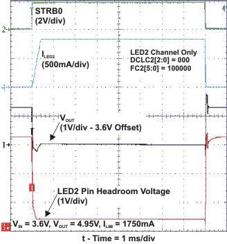
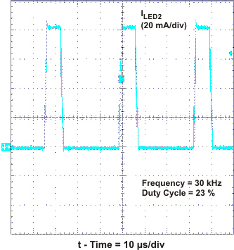 Figure 64. Low-Light Dimming Mode Operation
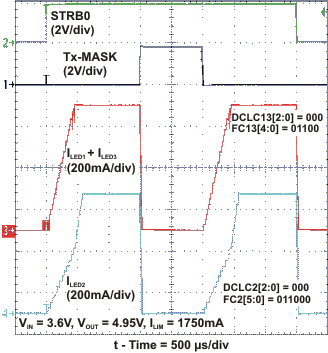
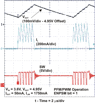 Figure 66. PFM Operation
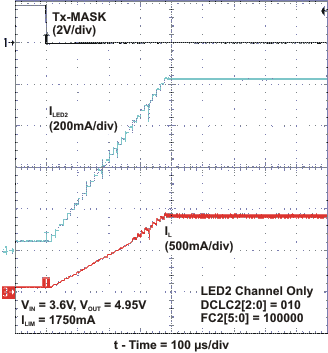
| STRB1 = 0 |
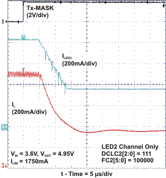
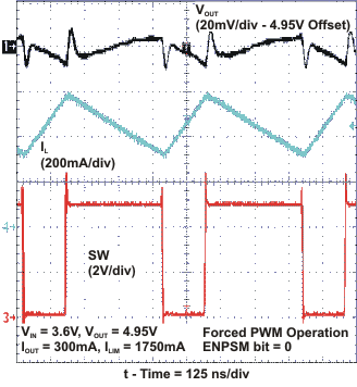 Figure 65. PWM Operation
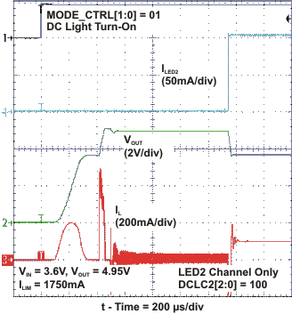 Figure 67. Start-Up Into Video Light Operation
10.2.2 1200-mA High Power White LED Solution Featuring Voltage Mode
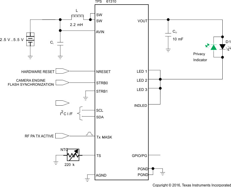 Figure 68. 1200-mA High Power White LED Solution Featuring Voltage Mode
10.2.2.1 Design Requirements
TPS6131x operates in standard voltage-boost regulator by setting mode-control bit MODE_CTRL[1:0] = 11. The LED current sink is turned off in this mode, with VIN = 2.5 V to 5.5 V, VOUT = 4.95 V, operating frequency 2 MHz.
10.2.2.2 Application Curves
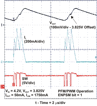 Figure 69. Down-Mode Operation (Voltage Mode)
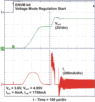 Figure 71. Start-Up Into Voltage Mode Operation
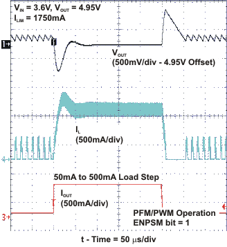 Figure 70. Voltage Mode Load Transient Response