SLVSEE7B June 2018 – January 2021 TPS61372
PRODUCTION DATA
- 1 Features
- 2 Applications
- 3 Description
- 4 Revision History
- 5 Pin Configuration and Functions
- 6 Specifications
- 7 Detailed Description
-
8 Application and Implementation
- 8.1 Application Information
- 8.2
Typical Application
- 8.2.1 Design Requirements
- 8.2.2
Detailed Design Procedure
- 8.2.2.1 Custom Design With WEBENCH® Tools
- 8.2.2.2 Setting the Output Voltage
- 8.2.2.3 Selecting the Inductor
- 8.2.2.4 Selecting the Output Capacitors
- 8.2.2.5 Selecting the Input Capacitors
- 8.2.2.6 Loop Stability and Compensation
- 8.2.2.7 Loop Compensation Design Steps
- 8.2.2.8 Selecting the Bootstrap Capacitor
- 8.2.3 Application Curves
- 9 Power Supply Recommendations
- 10Layout
- 11Device and Documentation Support
- 12Mechanical, Packaging, and Orderable Information
Package Options
Refer to the PDF data sheet for device specific package drawings
Mechanical Data (Package|Pins)
- YKB|16
Thermal pad, mechanical data (Package|Pins)
Orderable Information
3 Description
The TPS61372 is a full-integrated synchronous boost converter with the load disconnect built-in. The device supports output voltage up to 16 V with a 3.8-A current limit. The input voltage ranges from 2.5-V to 5.5-V supporting applications powered by a single-cell Lithium-ion battery or 5-V bus.
The TPS61372 uses the peak current mode with the adaptive off-time control topology. The device works in PWM operation of 1.5 MHz at moderate-to-heavy loads. At the light load conditions, the device can be configured in either auto PFM or forced PWM operation by the MODE pin connection. Auto PFM mode has the benefit of high efficiency at light load while forced PWM operation keeps the switching frequency constant across the whole load range. The TPS61372 has a soft start to minimize the inrush current during start-up. The TPS61372 features of the load disconnect during shut down and provides a output short protection of hiccup mode. In addition, the device implements output overvoltage and thermal shutdown protection. The TPS61372 delivers a compact solution size with a 16-pin WCSP 1.57-mm × 1.52-mm package of 0.5-mm height.
| PART NUMBER | PACKAGE(1) | BODY SIZE (NOM) |
|---|---|---|
| TPS61372 | DSBGA (16) | 1.57 mm × 1.52 mm |
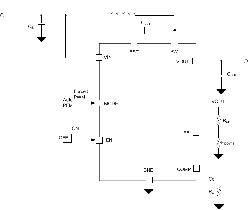
 Typical Application
Circuit