SLVSEE7B June   2018  – January 2021 TPS61372

PRODUCTION DATA  

  1. Features
  2. Applications
  3. Description
  4. Revision History
  5. Pin Configuration and Functions
  6. Specifications
    1. 6.1 Absolute Maximum Ratings
    2. 6.2 ESD Ratings
    3. 6.3 Recommended Operating Conditions
    4. 6.4 Thermal Information
    5. 6.5 Electrical Characteristics
    6. 6.6 Typical Characteristics
  7. Detailed Description
    1. 7.1 Overview
    2. 7.2 Functional Block Diagram
    3. 7.3 Feature Description
      1. 7.3.1 Undervoltage Lockout
      2. 7.3.2 Enable and Disable
      3. 7.3.3 Error Amplifier
      4. 7.3.4 Bootstrap Voltage (BST)
      5. 7.3.5 Load Disconnect
      6. 7.3.6 Overvoltage Protection
      7. 7.3.7 Thermal Shutdown
      8. 7.3.8 Start-Up
      9. 7.3.9 Short Protection
    4. 7.4 Device Functional Modes
      1. 7.4.1 Operation
      2. 7.4.2 Auto PFM Mode
      3. 7.4.3 Forced PWM Mode
      4. 7.4.4 Mode Selectable
  8. Application and Implementation
    1. 8.1 Application Information
    2. 8.2 Typical Application
      1. 8.2.1 Design Requirements
      2. 8.2.2 Detailed Design Procedure
        1. 8.2.2.1 Custom Design With WEBENCH® Tools
        2. 8.2.2.2 Setting the Output Voltage
        3. 8.2.2.3 Selecting the Inductor
        4. 8.2.2.4 Selecting the Output Capacitors
        5. 8.2.2.5 Selecting the Input Capacitors
        6. 8.2.2.6 Loop Stability and Compensation
          1. 8.2.2.6.1 Small Signal Model
        7. 8.2.2.7 Loop Compensation Design Steps
        8. 8.2.2.8 Selecting the Bootstrap Capacitor
      3. 8.2.3 Application Curves
  9. Power Supply Recommendations
  10. 10Layout
    1. 10.1 Layout Guidelines
    2. 10.2 Layout Example
      1. 10.2.1 Thermal Considerations
  11. 11Device and Documentation Support
    1. 11.1 Device Support
      1. 11.1.1 Third-Party Products Disclaimer
      2. 11.1.2 Development Support
        1. 11.1.2.1 Custom Design With WEBENCH® Tools
    2. 11.2 Receiving Notification of Documentation Updates
    3. 11.3 Support Resources
    4. 11.4 Trademarks
    5. 11.5 Electrostatic Discharge Caution
    6. 11.6 Glossary
  12. 12Mechanical, Packaging, and Orderable Information

Package Options

Refer to the PDF data sheet for device specific package drawings

Mechanical Data (Package|Pins)
  • YKB|16
Thermal pad, mechanical data (Package|Pins)
Orderable Information

Application Curves

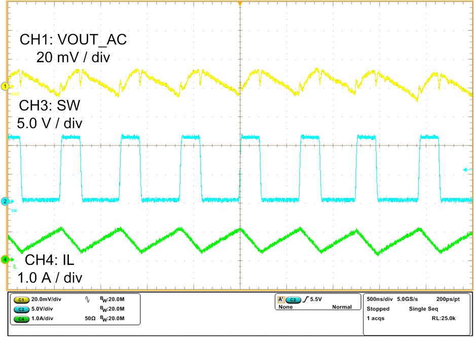
Typical condition VIN = 3 V to 5 V, VOUT = 12 V, temperature = 25°C, unless otherwise noted
GUID-09D6DC80-FF0D-41B6-A945-168936C69B66-low.png
VIN = 4 V VOUT = 12 V Mode = Auto PFM
L = 2.2 µH COUT = 3 × 10 µF
Figure 8-3 Steady-State at 200-mA Load
GUID-7B932A39-6CD0-40F5-9B4F-12841536DF75-low.png
VIN = 4 V VOUT = 12 V Mode = Auto PFM
L = 2.2 µH COUT = 3 × 10 µF
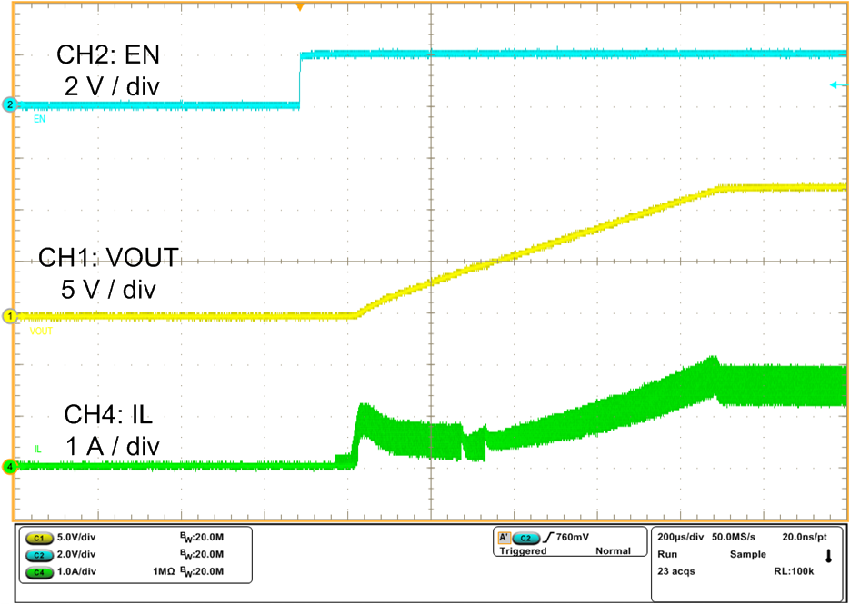
Figure 8-5 Start-Up by EN, Load = 12.5 Ω
GUID-85D86ED8-128A-45E6-8D51-58319BD0D449-low.png
VIN = 4 V VOUT = 12 V Mode = Auto PFM
L = 2.2 µH COUT = 3 × 10 µF
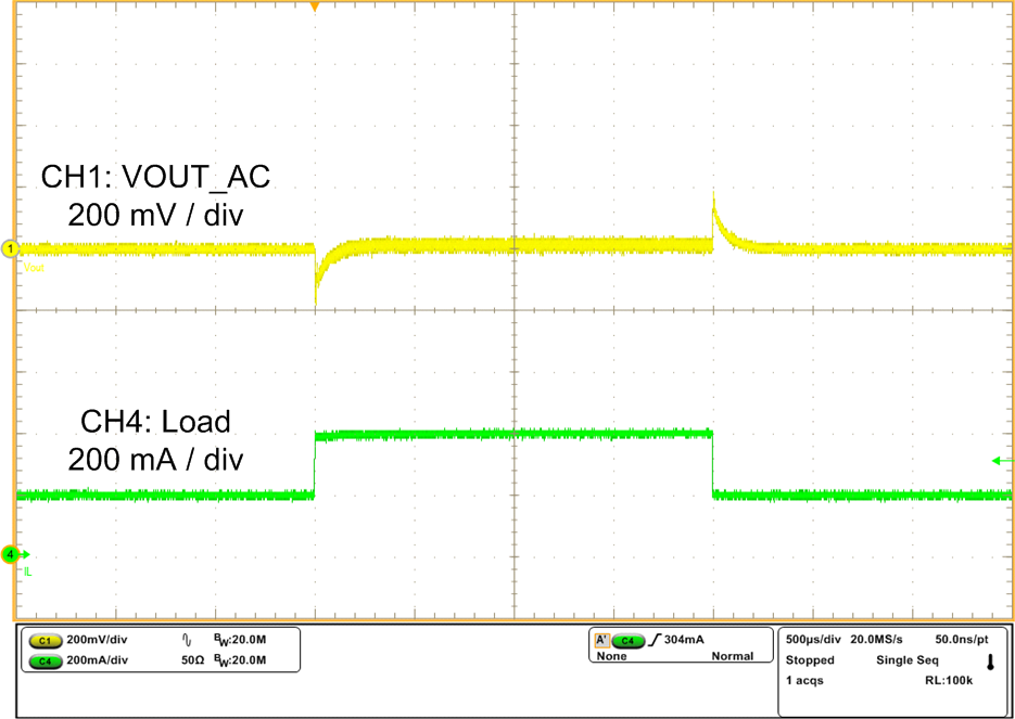
Figure 8-7 Load Transient, 200 mA to 400 mA, 100 mA / µs
GUID-5B52D747-80BE-41E5-83EC-7182B3015B99-low.png
VIN = 4 V VOUT = 12 V Mode = Auto PFM
L = 2.2 µH COUT = 3 × 10 µF
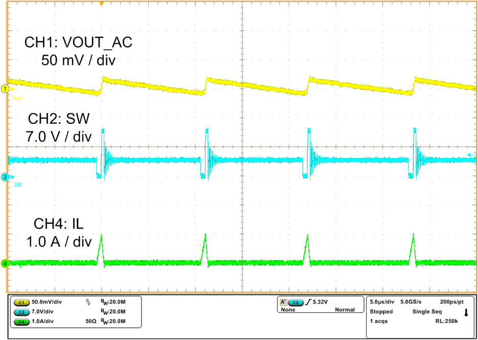
Figure 8-4 Steady-State at 10-mA Load
GUID-08BDD54C-9643-4ED4-8E0E-FC5CB079DEC8-low.png
VIN = 4 V VOUT = 12 V Mode = Auto PFM
L = 2.2 µH COUT = 3 × 10 µF
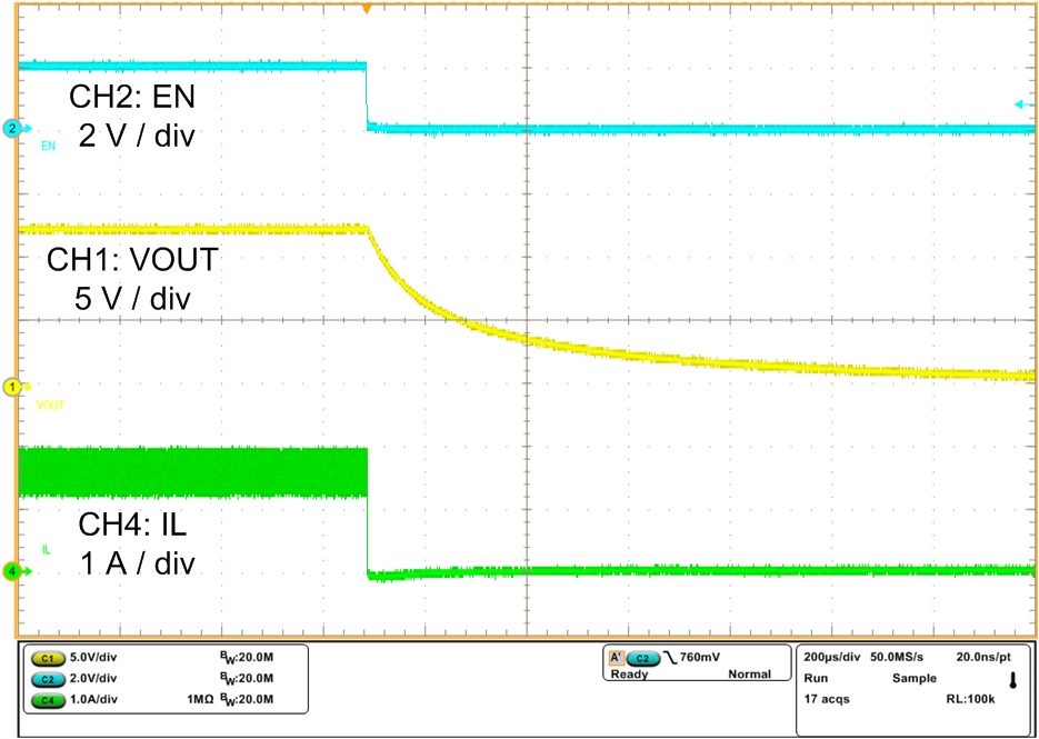
Figure 8-6 Shutdown by EN, Load = 12.5 Ω
GUID-4BB0DE51-2C9F-4E00-8443-CD9C87CCEAB8-low.png
VIN = 4 V VOUT = 12 V Mode = Auto PFM
L = 2.2 µH COUT = 3 × 10 µF
Figure 8-8 Shorted Output