SLVSFE7 November 2019 TPS61391
PRODUCTION DATA.
- 1 Features
- 2 Applications
- 3 Description
- 4 Revision History
- 5 Pin Configuration and Functions
- 6 Specifications
- 7 Detailed Description
-
8 Application and Implementation
- 8.1 Application Information
- 8.2
Typical Application
- 8.2.1 Design Requirement
- 8.2.2
Detailed Design Procedure
- 8.2.2.1 Selecting the Rectifier Diode
- 8.2.2.2 Selecting the Inductor
- 8.2.2.3 Selecting Output Capacitor
- 8.2.2.4 Selecting Filter Resistor and Capacitor
- 8.2.2.5 Setting the Output Voltage
- 8.2.2.6 Selecting Capacitor for CAP pin
- 8.2.2.7 Selecting Capacitor for AVCC pin
- 8.2.2.8 Selecting Capacitor for APD pin
- 8.2.2.9 Selecting the Resistors of MON1 or MON2
- 8.2.2.10 Selecting the Capacitors of MON1 or MON2
- 8.2.2.11 Selecting the Short Current Limit
- 8.2.3 Application Curves
- 9 Power Supply Recommendations
- 10Layout
- 11Device and Documentation Support
- 12Mechanical, Packaging, and Orderable Information
Package Options
Mechanical Data (Package|Pins)
- RTE|16
Thermal pad, mechanical data (Package|Pins)
- RTE|16
Orderable Information
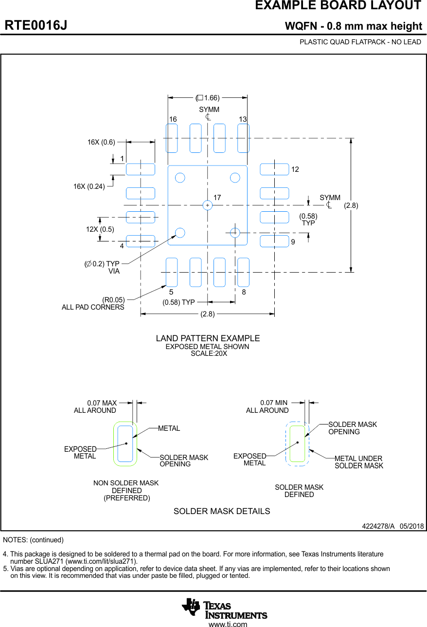
12 Mechanical, Packaging, and Orderable Information
The following pages include mechanical, packaging, and orderable information. This information is the most current data available for the designated devices. This data is subject to change without notice and revision of this document. For browser-based versions of this data sheet, refer to the left-hand navigation.


