SLVS893F December 2008 – May 2019 TPS61500
PRODUCTION DATA.
- 1 Features
- 2 Applications
- 3 Description
- 4 Revision History
- 5 Pin Configuration and Functions
- 6 Specifications
- 7 Detailed Description
-
8 Application and Implementation
- 8.1 Application Information
- 8.2
Typical Applications
- 8.2.1
Analog Dimming Method
- 8.2.1.1 Design Requirements
- 8.2.1.2
Detailed Design Procedure
- 8.2.1.2.1 Programming the Overvoltage Protection
- 8.2.1.2.2 Programming the LED Current
- 8.2.1.2.3 Implementing Dimming
- 8.2.1.2.4 Computing the Maximum Output Current
- 8.2.1.2.5 Selecting the Inductor
- 8.2.1.2.6 Selecting the Schottky Diode
- 8.2.1.2.7 Selecting the Compensation Capacitor and Resistor
- 8.2.1.2.8 Selecting the Input and Output Capacitor
- 8.2.1.3 Application Curves
- 8.2.2 Pure PWM Dimming Method
- 8.2.1
Analog Dimming Method
- 9 Power Supply Recommendations
- 10Layout
- 11Device and Documentation Support
- 12Mechanical, Packaging, and Orderable Information
Package Options
Mechanical Data (Package|Pins)
- PWP|14
Thermal pad, mechanical data (Package|Pins)
Orderable Information
7.3.1 Switching Frequency
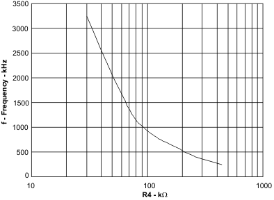
The switch frequency is determined by a resistor connected to the FREQ pin of the TPS61500. Do not leave this pin open. A resistor must always be connected for proper operation. See Table 2 and Figure 6 for resistor values and corresponding frequencies.
Table 2. Switching Frequency vs External Resistor
| R4 (kΩ) | fSW (kHz) |
|---|---|
| 443 | 240 |
| 256 | 400 |
| 176 | 600 |
| 80 | 1200 |
| 51 | 2000 |
 Figure 6. Switching Frequency vs External Resistor
 Increasing switching frequency reduces the value of external capacitors and inductors, but also reduces the power conversion efficiency. The user must set the frequency for compromise between efficiency and solution size.