SLVSC55C August 2013 – November 2021 TPS62090-Q1
PRODUCTION DATA
- 1 Features
- 2 Applications
- 3 Description
- 4 Revision History
- 5 Pin Configuration and Functions
- 6 Specifications
-
7 Detailed Description
- 7.1 Overview
- 7.2 Functional Block Diagram
- 7.3
Feature Description
- 7.3.1 Enable and Disable (EN)
- 7.3.2 Soft Start (SS) and Hiccup Current Limit During Start-Up
- 7.3.3 Voltage Tracking (SS)
- 7.3.4 Short-Circuit Protection (Hiccup Mode)
- 7.3.5 Output Discharge Function
- 7.3.6 Power Good Output (PG)
- 7.3.7 Frequency Set Pin (FREQ)
- 7.3.8 Undervoltage Lockout (UVLO)
- 7.3.9 Thermal Shutdown
- 7.3.10 Charge Pump (CP, CN)
- 7.4 Device Functional Modes
- 8 Application and Implementation
- 9 Power Supply Recommendations
- 10Layout
- 11Device and Documentation Support
- 12Mechanical, Packaging, and Orderable Information
Package Options
Mechanical Data (Package|Pins)
- RGT|16
Thermal pad, mechanical data (Package|Pins)
- RGT|16
Orderable Information
7.3.3 Voltage Tracking (SS)
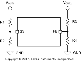
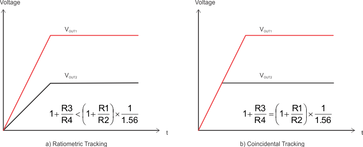
The SS pin is externally driven by another voltage source to achieve output voltage tracking. The application circuit is shown in Figure 7-1. The internal reference voltage follows the voltage at the SS pin with a fraction of 1.56 until the internal reference voltage of 0.8 V is reached. The device achieves ratiometric or coincidental (simultaneous) output tracking, as shown in Figure 7-2.
 Figure 7-1 Output Voltage Tracking
 Figure 7-2 Voltage Tracking Options
The R2 value should be set properly to achieve accurate voltage tracking by taking 7.5-µA soft start-up current into account. 1 kΩ or smaller is a sufficient value for R2.
For decreasing the SS pin voltage, the device does not sink current from the output when the device is in power save mode. So the resulting decreases of the output voltage may be slower than the SS pin voltage if the load is light. When driving the SS pin with an external voltage, do not exceed the voltage rating of the SS pin which is
7 V.