SLVSDZ7A September   2017  – December 2017 TPS62097-Q1

PRODUCTION DATA.  

  1. Features
  2. Applications
  3. Description
    1.     Device Images
      1.      1.8-V Output, Typical Application
      2.      1.8-V Output, Efficiency, MODE = Open
  4. Revision History
  5. Terminal Configuration and Functions
    1.     Pin Functions
  6. Specifications
    1. 6.1 Absolute Maximum Ratings
    2. 6.2 ESD Ratings
    3. 6.3 Recommend Operating Conditions
    4. 6.4 Thermal Information
    5. 6.5 Electrical Characteristics
    6. 6.6 Typical Characteristics
  7. Detailed Description
    1. 7.1 Overview
    2. 7.2 Functional Block Diagram
    3. 7.3 Feature Description
      1. 7.3.1 100% Duty Cycle Mode
      2. 7.3.2 Switch Current Limit and Hiccup Short Circuit Protection
      3. 7.3.3 Under Voltage Lockout (UVLO)
      4. 7.3.4 Thermal Shutdown
    4. 7.4 Device Function Modes
      1. 7.4.1 Enable and Disable (EN)
      2. 7.4.2 Power Save Mode and Forced PWM Mode (MODE)
      3. 7.4.3 Soft Startup (SS/TR)
      4. 7.4.4 Voltage Tracking (SS/TR)
      5. 7.4.5 Power Good (PG)
  8. Application Information
    1. 8.1 Application Information
    2. 8.2 1.8-V Output Application
      1. 8.2.1 Design Requirements
      2. 8.2.2 Detailed Design Procedure
        1. 8.2.2.1 Setting the Output Voltage
        2. 8.2.2.2 Output Filter Design
        3. 8.2.2.3 Inductor Selection
        4. 8.2.2.4 Capacitor Selection
      3. 8.2.3 Application Performance Curves
  9. Power Supply Recommendations
  10. 10PCB Layout
    1. 10.1 Layout Guidelines
    2. 10.2 Layout Example
    3. 10.3 Thermal Information
  11. 11Device and Documentation Support
    1. 11.1 Device Support
      1. 11.1.1 Third-Party Products Disclaimer
    2. 11.2 Community Resources
    3. 11.3 Trademarks
    4. 11.4 Electrostatic Discharge Caution
    5. 11.5 Glossary
  12. 12Mechanical, Packaging, and Orderable Information

Package Options

Mechanical Data (Package|Pins)
Thermal pad, mechanical data (Package|Pins)
Orderable Information

Application Performance Curves

TA = 25°C, BOM = Table 4 unless otherwise noted.

TPS62097-Q1 D001_SLVSDZ7_TPS62097Q.gif
VOUT = 1.0 V FSW = 2.0 MHz
Figure 7. Efficiency
TPS62097-Q1 D003_SLVSDZ7_TPS62097Q.gif
VOUT = 1.8 V FSW = 2.0 MHz
Figure 9. Efficiency
TPS62097-Q1 D005_SLVSDZ7_TPS62097Q.gif
VOUT = 3.3 V FSW = 2.0 MHz
Figure 11. Efficiency
TPS62097-Q1 D006_SLVSDZ7_TPS62097Q.gif
Figure 13. Load Regulation
TPS62097-Q1 D008_SLVSDZ7_TPS62097Q.gif
VOUT = 1.0 V RMode = 8.2 kΩ
Figure 15. Switching Frequency, Forced PWM Mode (1.5 MHz)
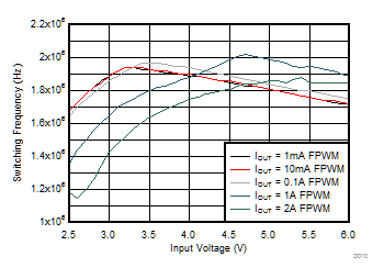
TPS62097-Q1 D010_SLVSDZ7_TPS62097Q.gif
VOUT = 1.0 V MODE = Open
Figure 17. Switching Frequency, Forced PWM Mode (2.5MHz)
TPS62097-Q1 D017_SLVSCD6_TPS62097.gif
VOUT = 1.2 V IOUT = 30 mA
Figure 19. Output Ripple, PSM Operation
TPS62097-Q1 D019_SLVSCD6_TPS62097.gif
VOUT = 1.2 V IOUT = 0 A to 2 A, 1A / µs
Figure 21. Load Transient, Forced PWM Mode (2.0MHz)
TPS62097-Q1 D021_SLVSCD6_TPS62097.gif
VOUT = 1.2 V ROUT = 0.6 Ω (2 A)
Figure 23. Startup and Shutdown with Load
TPS62097-Q1 D002_SLVSDZ7_TPS62097Q.gif
VOUT = 1.2 V FSW = 2.0 MHz
Figure 8. Efficiency
TPS62097-Q1 D004_SLVSDZ7_TPS62097Q.gif
VOUT = 2.5 V FSW = 2.0 MHz
Figure 10. Efficiency
TPS62097-Q1 D016_SLVSDZ7_TPS62097Q.gif
VOUT = 1.8 V VIN = 5.0 V
Figure 12. Efficiency with Different Switching Frequency
TPS62097-Q1 D007_SLVSDZ7_TPS62097Q.gif
Figure 14. Line Regulation
TPS62097-Q1 D009_SLVSDZ7_TPS62097Q.gif
VOUT = 1.0 V MODE = AGND, Forced PWM
Figure 16. Switching Frequency, Forced PWM Mode (2.0MHz)
TPS62097-Q1 D016_SLVSCD6_TPS62097.gif
VOUT = 1.2 V IOUT = 2 A
Figure 18. Output Ripple, PWM Operation (2.0MHz)
TPS62097-Q1 D018_SLVSCD6_TPS62097.gif
VOUT = 1.2 V IOUT = 0 A to 2 A, 1A / µs
Figure 20. Load Transient, PWM/PSM Mode (2.0MHz)
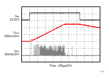
TPS62097-Q1 D020_SLVSCD6_TPS62097.gif
VOUT = 1.2 V ROUT = No Load
Figure 22. Startup and Shutdown without Load
TPS62097-Q1 D022_SLVSCD6_TPS62097.gif
VOUT = 1.2 V ROUT = 0.8 Ω (1.5 A) with 1-ms short
Figure 24. Short Circuit Protection, HICCUP