SLVS585E July 2005 – June 2015 TPS62110 , TPS62111 , TPS62112 , TPS62113
PRODUCTION DATA.
- 1 Features
- 2 Applications
- 3 Description
- 4 Typical Application Schematic
- 5 Revision History
- 6 Device Comparison Table
- 7 Pin Configuration and Functions
- 8 Specifications
- 9 Detailed Description
- 10Application and Implementation
- 11Power Supply Recommendations
- 12Layout
- 13Device and Documentation Support
- 14Mechanical, Packaging, and Orderable Information
Package Options
Mechanical Data (Package|Pins)
- RSA|16
Thermal pad, mechanical data (Package|Pins)
- RSA|16
Orderable Information
10 Application and Implementation
NOTE
Information in the following applications sections is not part of the TI component specification, and TI does not warrant its accuracy or completeness. TI’s customers are responsible for determining suitability of components for their purposes. Customers should validate and test their design implementation to confirm system functionality.
10.1 Application Information
The TPS6211x devices are a family of low-noise synchronous step-down DC-DC converters that are ideally suited for systems powered from a 2- to 4-cell Li-ion battery or from a 12-V or 15-V rail.
10.2 Typical Applications
10.2.1 Standard Connection for Adjustable Version
10.2.1.1 Design Requirements
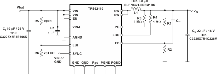
The design guidelines provide a component selection to operate the device within the Recommended Operating Conditions.
Table 1. Bill of Materials for the Adjustable Version
| REFERENCE | PART NUMBER | VALUE | MANUFACTURER |
|---|---|---|---|
| Ci | C3225X5R1E106K | 10 µF | TDK |
| Co | C3225X7R1C226M | 22 µF | TDK |
| L1 | SLF7032T-6R8M1R6 | 6.8 µH | TDK |
| C1 | TMK212B7105KG-T | 1 µF | Taiyo Yuden |
| IC1 | TPS62110 | - | Texas Instruments |
| R1 | generic metal film resistor; tolerance 1% | 220 kΩ (depending on desired output voltage) | — |
| R2 | generic metal film resistor; tolerance 1% | 390 kΩ (depending on desired output voltage) | — |
| R3, R4 | generic metal film resistor; tolerance 1% | 1 MΩ | — |
| R5 | generic metal film resistor; tolerance 1% | open | — |
| R6 | generic metal film resistor; tolerance 1% | 261 kΩ | — |
| C(ff) | generic ceramic capacitor; COG | 10 pF (depending on output voltage) | — |
10.2.1.2 Detailed Design Procedure
The graphs were generated using the EVM with the setup according to Figure 6, unless otherwise noted. Graphs for an output voltage of 1.5 V and 1.8 V were generated using the TPS62110 device with the output voltage dividers adjusted according Table 2.

Table 2. Recommended Resistors
| OUTPUT VOLTAGE | R1 | R2 | NOMINAL VOLTAGE | TYPICAL Cff |
|---|---|---|---|---|
| 9 V | 680 kΩ | 100 kΩ | 8.993 V | 22 pF |
| 5 V | 510 kΩ | 150 kΩ | 5.073 V | 10 pF |
| 3.3 V | 560 kΩ | 300 kΩ | 3.305 V | 10 pF |
| 2.5 V | 390 kΩ | 330 kΩ | 2.515 V | 10 pF |
| 1.8 V | 220 kΩ | 390 kΩ | 1.803 V | 10 pF |
| 1.5 V | 100 kΩ | 330 kΩ | 1.502 V | 10 pF |
10.2.1.2.1 External Component Selection
The control loop of the TPS6211x family of devices requires a certain value for the output inductor and the output capacitor for stable operation. As long as the nominal value of L × C ≥ 6.2 µH × 22 µF, the control loop has enough phase margin and the device is stable. Reducing the inductor value without increasing the output capacitor (or vice versa) may cause stability problems. There are applications where it may be useful to increase the value of the output capacitor, and so on, for a low-transient output-voltage change. From a stability point of view, the inductor value could be decreased to keep the L × C product constant. However, there are drawbacks if the inductor value is decreased. A low inductor value causes a high inductor ripple current, and therefore reduces the maximum DC output current. Table 3 gives the advantages and disadvantages when designing the inductor and output capacitor.
Table 3. Advantages and Disadvantages When Designing the Inductor and Output Capacitor
| INFLUENCE ON STABILITY | ADVANTAGE | DISADVANTAGE | |
|---|---|---|---|
| Increase Cout (>22 µF) | Uncritical | Less output voltage ripple | None |
| Less output voltage overshoot / undershoot during load transient | |||
| Decrease Cout (<22 µF) | Critical Increase inductor value >6.8 µH also |
None | Higher-output voltage ripple |
| High-output voltage overshoot / undershoot during load transient | |||
| Less gain and phase margin | |||
| Increase L (>6.8 µH) | Uncritical | Less inductor current ripple | More energy stored in the inductor → higher voltage overshoot during load transient |
| Higher DC output current possible if operated close to the current limit | Smaller current rise → higher voltage undershoot during load transient → do not decrease the value of Cout due to these effects | ||
| Decrease L (<6.8 µH) | Critical | Small voltage overshoot and undershoot during load transient | High inductor current ripple especially at high input voltage and low output voltage |
| Increase output capacitor value > 22 µF also |
10.2.1.2.2 Inductor Selection
As shown in Table 3, the inductor value can be increased to greater values. For good performance, the peak-to-peak inductor-current ripple should be less than 30% of the maximum DC output current. Especially at input voltages greater than 12 V, it makes sense to increase the inductor value to keep the inductor-current ripple low. In such applications, the inductor value can be increased to 10 µH or 22 µH. Values greater than 22 µH should be avoided to keep the voltage overshoot during load transient in an acceptable range.
After choosing the inductor value, two additional inductor parameters should be considered:
- Current rating of the inductor
- DC resistance

where
- f = Switching frequency (1000 kHz typical)
- L = Inductor value
- ΔIL = Peak-to-peak inductor ripple current
- IL(max) = Maximum inductor current
The highest inductor current occurs at maximum VI. A more conservative approach is to select the inductor current rating just for the maximum switch current of the TPS6211x, which is 2.4 A (typically). See Table 4 for recommended inductors.
Table 4. List of Inductors
| MANUFACTURER | PART NO. | INDUCTANCE | DC RESISTANCE | SATURATION CURRENT |
|---|---|---|---|---|
| Coilcraft | MSS6132-682 | 6.8 µH | 65 mΩ (maximum) | 1.5 A |
| HA3808-AL | 6.8 µH | 99 mΩ (typical) | 4.4 A | |
| Epcos | B82462G4682M | 6.8 µH | 50 mΩ (maximum) | 1.5 A |
| Sumida | CDRH5D28-6R2 | 6.2 µH | 33 mΩ (typical) | 1.8 A |
| TDK | SLF6028T-6R8M1R5 | 6.8 µH | 35 mΩ (typical) | 1.5 A |
| SLF7032T-6R8M1R6 | 6.8 µH | 41 mΩ (typical) | 1.6 A | |
| Wurth | 7447789006 | 6.8 µH | 44 mΩ (typical) | 2.75 A |
| 7447779006 | 6.8 µH | 33 mΩ (typical) | 3.3 A | |
| 744053006 | 6.2 µH | 45 mΩ (typical) | 1.8 A |
10.2.1.2.3 Output Capacitor Selection
A 22-μF (typical) output capacitor is needed with a 6.8-μH inductor. For an output voltage greater than 5 V, a 33-μF (minimum) output capacitor is required for stability. For best performance, a low-ESR ceramic output capacitor is needed.
The RMS ripple current is calculated using Equation 5.

The overall output ripple voltage is the sum of the voltage spike caused by the output capacitor ESR plus the voltage ripple caused by charging and discharging the output capacitor:

where
- the highest output voltage ripple occurs at the highest input voltage VI.
10.2.1.2.4 Input Capacitor Selection
The nature of the buck converter is a pulsating input current; therefore, a low ESR input capacitor is required for best input voltage filtering and for minimizing the interference with other circuits caused by high input voltage spikes. The input capacitor should have a minimum value of 10 µF and can be increased without any limit for better input voltage filtering. The input capacitor should be rated for the maximum input ripple current and is calculated using Equation 7.

The worst-case RMS ripple current occurs at D = 0.5 and is calculated as: IRMS = IO/2. Ceramic capacitors show a good performance because of their low ESR value, and they are less sensitive against voltage transients compared to tantalum capacitors. Place the input capacitor as close as possible to the VIN and PGND pins of the IC for best performance.
An additional 1-µF input capacitor is required from VINA to AGND. VIN and VINA must be connected to the same source. TI does not recommend an RC filter from VIN to VINA.
10.2.1.2.5 Feedforward Capacitor Selection
The feedforward capacitor (Cff) is needed to compensate for parasitic capacitance from the feedback pin to GND. Typically, a value of 4.7 pF to 22 pF is needed for an output voltage divider with a equivalent resistance (R1 in parallel with R2) in the 150-kΩ range. The value can be chosen based on best transient performance and lowest output voltage ripple in PFM mode.
10.2.1.2.6 Recommended Capacitors
TI recommends using only X5R or X7R ceramic capacitors as input and output capacitors. Ceramic capacitors show a DC-bias effect. This effect reduces the effective capacitance when a DC-bias voltage is applied across a ceramic capacitor, as on the output and input capacitor of a DC-DC converter. The effect may lead to a significant capacitance drop, especially for high input and output voltages and small capacitor packages. See the manufacturer's data sheet about the performance with a DC bias voltage applied. It may be necessary to choose a higher voltage rating or nominal capacitance value to get the required value at the operating point. The capacitors listed in Table 5 have been tested with the TPS6211x devices with good performance.
Table 5. List of Capacitors
| MANUFACTURER | PART NUMBER | SIZE | VOLTAGE | CAPACITANCE | TYPE |
|---|---|---|---|---|---|
| Taiyo Yuden | TMK316BJ106KL | 1206 | 25 V | 10 µF | Ceramic |
| EMK325BJ226KM | 1210 | 16 V | 22 µF | ||
| TDK | C3225X5R1E106M | 1210 | 25 V | 10 µF | Ceramic |
| C3225X7R1C226M | 16 V | 22 µF | |||
| C3216X5R1E106MT | 1206 | 25 V | 10 µF |
10.2.1.3 Application Curves
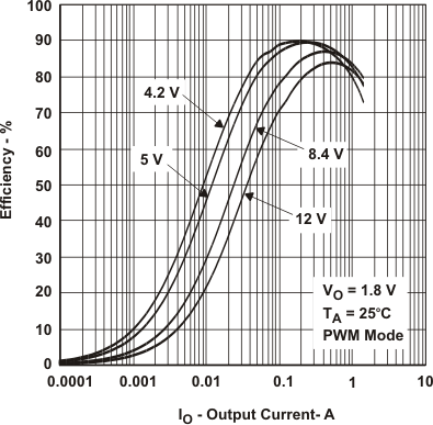 Figure 7. TPS62110 Efficiency vs Output Current
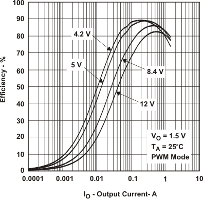 Figure 9. TPS62110 Efficiency vs Output Current
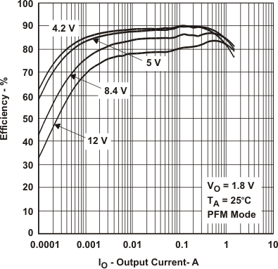 Figure 8. TPS62110 Efficiency vs Output Current
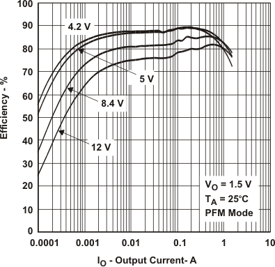 Figure 10. TPS62110 Efficiency vs Output Current
10.2.2 Standard Connection for Fixed-Voltage Version
10.2.2.1 Design Requirements
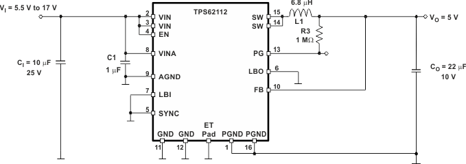
The design guidelines provide a component selection to operate the device within the Recommended Operating Conditions.
Table 6. Bill of Materials for the Fixed Voltage Versions
| REFERENCE | PART NUMBER | VALUE | MANUFACTURER |
|---|---|---|---|
| Ci | C3225X5R1E106K | 10 µF | TDK |
| Co | C3225X7R1C226M | 22 µF | TDK |
| L1 | SLF7032T-6R8M1R6 | 6.8 µH | TDK |
| C1 | TMK212B7105KG-T | 1 µF | Taiyo Yuden |
| IC1 | TPS62112 | — | Texas Instruments |
| R3 | generic metal film resistor; tolerance 1% | 1 MΩ | — |
10.2.2.2 Detailed Design Procedure
The graphs were generated using the EVM with the setup according to Figure 6, unless otherwise noted. Graphs for an output voltage of 5 V and 3.3 V were generated using the TPS62111 and TPS62112 devices with R1 = 0 Ω and R2 = open.
10.2.2.3 Application Curves
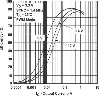
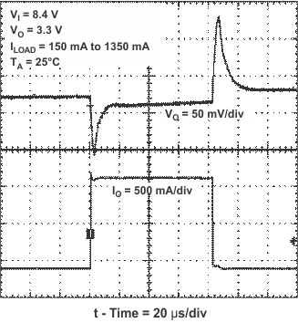
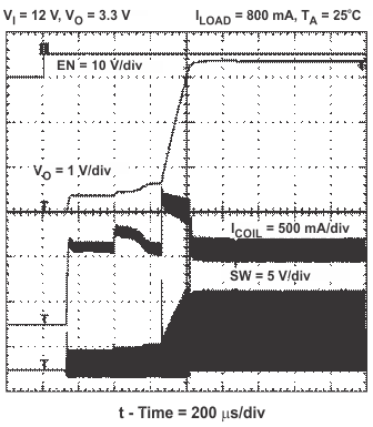
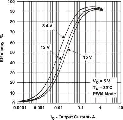 Figure 12. TPS62112 Efficiency vs Output Current
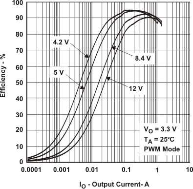 Figure 14. TPS62111 Efficiency vs Output Current
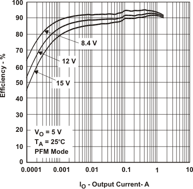 Figure 13. TPS62112 Efficiency vs Output Current
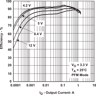 Figure 15. TPS62111 Efficiency vs Output Current
10.3 System Examples
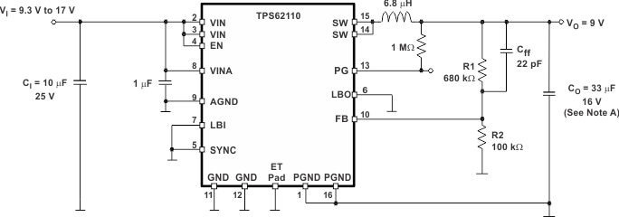
The TPS62110 device can be used within an adjustable output voltage range from 1.2 V to 16 V. Figure 21 shows and application example with 9-V output.
