SLVSAJ0F November   2011  – October 2021 TPS62140 , TPS62140A , TPS62141 , TPS62142 , TPS62143

PRODUCTION DATA  

  1. Features
  2. Applications
  3. Description
  4. Revision History
  5. Device Comparison Table
  6. Pin Configuration and Functions
  7. Specifications
    1. 7.1 Absolute Maximum Ratings (1)
    2. 7.2 ESD Ratings
    3. 7.3 Recommended Operating Conditions
    4. 7.4 Thermal Information
    5. 7.5 Electrical Characteristics
    6. 7.6 Typical Characteristics
  8. Detailed Description
    1. 8.1 Overview
    2. 8.2 Functional Block Diagrams
    3. 8.3 Feature Description
      1. 8.3.1 Enable/Shutdown (EN)
      2. 8.3.2 Soft-Start/Tracking (SS/TR)
      3. 8.3.3 Power Good (PG)
      4. 8.3.4 Pin-Selectable Output Voltage (DEF)
      5. 8.3.5 Frequency Selection (FSW)
      6. 8.3.6 Undervoltage Lockout (UVLO)
      7. 8.3.7 Thermal Shutdown
    4. 8.4 Device Functional Modes
      1. 8.4.1 Pulse-Width Modulation (PWM) Operation
      2. 8.4.2 Power Save Mode Operation
      3. 8.4.3 100% Duty-Cycle Operation
      4. 8.4.4 Current Limit and Short Circuit Protection
  9. Application and Implementation
    1. 9.1 Application Information
    2. 9.2 Typical Application
      1. 9.2.1 Design Requirements
      2. 9.2.2 Detailed Design Procedure
        1. 9.2.2.1 Programming the Output Voltage
        2. 9.2.2.2 External Component Selection
          1. 9.2.2.2.1 Inductor Selection
          2. 9.2.2.2.2 Capacitor Selection
            1. 9.2.2.2.2.1 Output Capacitor
            2. 9.2.2.2.2.2 Input Capacitor
            3. 9.2.2.2.2.3 Soft-Start Capacitor
        3. 9.2.2.3 Tracking Function
        4. 9.2.2.4 Output Filter and Loop Stability
      3. 9.2.3 Application Curves
    3. 9.3 System Examples
      1. 9.3.1 LED Power Supply
      2. 9.3.2 Active Output Discharge
      3. 9.3.3 Inverting Power Supply
      4. 9.3.4 Various Output Voltages
  10. 10Power Supply Recommendations
  11. 11Layout
    1. 11.1 Layout Guidelines
    2. 11.2 Layout Example
    3. 11.3 Thermal Considerations
  12. 12Device and Documentation Support
    1. 12.1 Device Support
      1. 12.1.1 Third-Party Products Disclaimer
    2. 12.2 Documentation Support
      1. 12.2.1 Related Documentation
    3. 12.3 Receiving Notification of Documentation Updates
    4. 12.4 Support Resources
    5. 12.5 Trademarks
    6. 12.6 Electrostatic Discharge Caution
    7. 12.7 Glossary
  13. 13Mechanical, Packaging, and Orderable Information

Package Options

Mechanical Data (Package|Pins)
Thermal pad, mechanical data (Package|Pins)
Orderable Information
Inductor Selection

The inductor selection is affected by several effects like inductor ripple current, output ripple voltage, PWM-to-PSM transition point, and efficiency. In addition, the inductor selected must be rated for appropriate saturation current and DC resistance (DCR). Equation 7 and Equation 8 calculate the maximum inductor current under static load conditions.

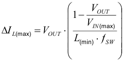
Equation 7. GUID-9A8BEC90-932E-4019-BD1C-E0101B7331AE-low.gif

Equation 8. GUID-2FC7D48A-5FFD-4E2B-8D7F-3CADD16C691A-low.gif

where

  • IL(max) is the maximum inductor current
  • ΔIL is the peak-to-peak inductor ripple current
  • L(min) is the minimum effective inductor value
  • fSW is the actual PWM switching frequency

Calculating the maximum inductor current using the actual operating conditions gives the minimum required inductor saturation current. It is recommended to add a margin of about 20%. A larger inductor value is also useful to get lower ripple current, but increases the transient response time and size as well. The following inductors have been used with the TPS6214x and are recommended for use:

Table 9-3 List of Inductors
TYPE INDUCTANCE (µH) CURRENT (A)(1) DIMENSIONS [L x B x H] (mm) MANUFACTURER(2)
XFL4020-222ME_ 2.2 µH, ±20% 3.5 4 x 4 x 2.1 Coilcraft
XFL4020-332ME_ 3.3 µH, ±20% 2.9 4 x 4 x 2.1 Coilcraft
IHLP1212BZ-11 2.2 µH, ±20% 3.0 3 x 3.6 x 2 Vishay
IHLP1616AB-11 2.2 µH, ±20% 2.75 4.05 x 4.45 x 1.2 Vishay
DEM4518C 1235AS-H-3R3M 3.3 µH, ±20% 2.5 4.5 x 4.7 x 1.9 Toko
Lower of IRMS at 40°C rise or ISAT at 30% drop.
See Third-Party Products disclaimer

The inductor value also determines the load current at which the power-save mode is entered:

Equation 9. GUID-4A535C30-3C3C-471A-9805-3E1766955FA3-low.gif

Using Equation 8, this current level can be adjusted by changing the inductor value.