SLVSAJ0F November 2011 – October 2021 TPS62140 , TPS62140A , TPS62141 , TPS62142 , TPS62143
PRODUCTION DATA
- 1 Features
- 2 Applications
- 3 Description
- 4 Revision History
- 5 Device Comparison Table
- 6 Pin Configuration and Functions
- 7 Specifications
- 8 Detailed Description
- 9 Application and Implementation
- 10Power Supply Recommendations
- 11Layout
- 12Device and Documentation Support
- 13Mechanical, Packaging, and Orderable Information
Package Options
Mechanical Data (Package|Pins)
- RGT|16
Thermal pad, mechanical data (Package|Pins)
- RGT|16
Orderable Information
3 Description
The TPS6214x family is an easy-to-use synchronous step-down DC-DC converter optimized for applications with high power density. A high switching frequency of typically 2.5 MHz allows the use of small inductors and provides fast transient response by use of the DCS-Control topology.
With their wide operating input voltage range of 3 V to 17 V, the devices are ideally suited for systems powered from either a Li-Ion or other batteries, as well as from 12-V intermediate power rails. It supports up to 2 A of continuous output current at output voltages between 0.9 V and 6 V (with 100% duty-cycle mode). The output voltage start-up ramp is controlled by the soft-start pin, which allows operation as either a standalone power supply or in tracking configurations. Power sequencing is also possible by configuring the Enable (EN) and open-drain Power Good (PG) pins.
In power save mode, the devices draw quiescent current of about 17 μA from VIN. Power Save Mode, entered automatically and seamlessly if the load is small, maintains high efficiency over the entire load range. In Shutdown Mode, the device is turned off and current consumption is less than 2 μA.
The device, available in adjustable and fixed output voltage versions, is packaged in a 16-pin VQFN package measuring 3 mm × 3 mm (RGT).
| PART NUMBER | PACKAGE(1) | BODY SIZE (NOM) |
|---|---|---|
| TPS6214x | VQFN (16) | 3.00 mm × 3.00 mm |
 Typical Application
Schematic
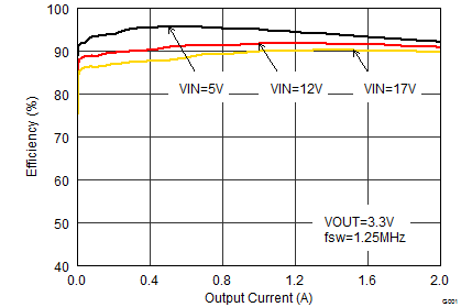
 Efficiency vs Output
Current