SLVSBB8B August 2014 – May 2017 TPS62180 , TPS62182
PRODUCTION DATA.
- 1 Features
- 2 Applications
- 3 Description
- 4 Revision History
- 5 Device Comparison Table
- 6 Pin Configuration and Functions
- 7 Specifications
-
8 Detailed Description
- 8.1 Overview
- 8.2 Functional Block Diagram
- 8.3 Feature Description
- 8.4
Device Functional Modes
- 8.4.1 Pulse Width Modulation (PWM) Operation
- 8.4.2 Power Save Mode (PSM) Operation
- 8.4.3 Minimum Duty Cycle and 100% Mode Operation
- 8.4.4 Automatic Efficiency Enhancement (AEE)
- 8.4.5 Phase-Shifted Operation
- 8.4.6 Current Limit, Current Balancing, and Short Circuit Protection
- 8.4.7 Tracking
- 8.4.8 Operation with Fixed VOUT
- 9 Application and Implementation
- 10Power Supply Recommendations
- 11Layout
- 12Device and Documentation Support
- 13Mechanical, Packaging, and Orderable Information
Package Options
Mechanical Data (Package|Pins)
- YZF|24
Thermal pad, mechanical data (Package|Pins)
Orderable Information
11 Layout
11.1 Layout Guidelines
The PCB layout of the TPS6218x demands careful attention to ensure proper operation, thermal profile, low noise emission and to achieve best performance. A poor layout can lead to issues like poor regulation, stability and accuracy weaknesses, increased EMI radiation and noise sensitivity. While the TPS6218x provides very high power density, the PCB layout also contributes significantly to the thermal performance.
11.1.1 PCB Layout
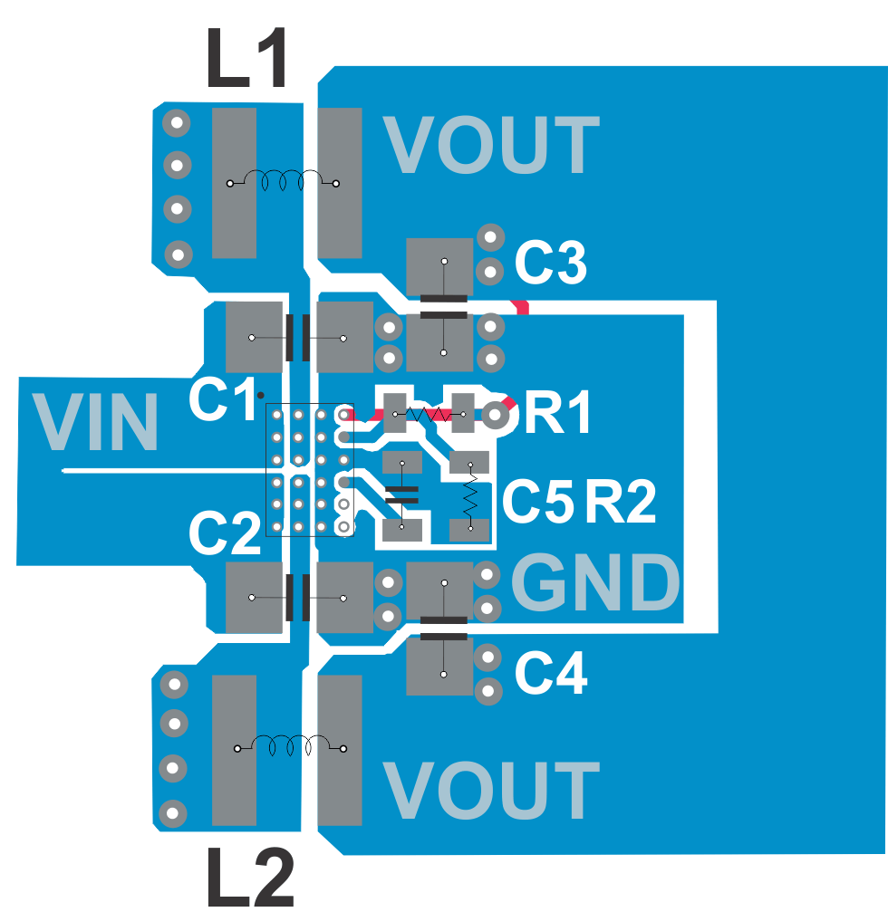
A recommended PCB layout for the TPS62180 dual phase solution is shown below. It ensures best electrical and optimized thermal performance considering the following important topics:
- The input capacitors must be placed as close as possible to the appropriate pins of the device. This provides low resistive and inductive paths for the high di/dt input current. The input capacitance is split, as is the VIN connection, to avoid interference between the input lines.
- The SW node connection from the IC to the inductor conducts high currents. It should be kept short and can be designed in parallel with an internal or bottom layer plane, to provide low resistance and enhanced thermal behavior.
- The VOUT regulation loop is closed with COUT and its ground connection. If a ground layer or plane is used, a direct connection by vias, as shown, is recommended. Otherwise the connection of COUT to GND must be short for good load regulation.
- The FB node is sensitive to dv/dt signals. Therefore the resistive divider should be placed close to the FB pin, avoiding long trace distance. Using the TPS62182 (fixed output voltage version), the FB pin can be left floating, but it is good practice and recommended to connect it to AGND for best thermal characteristics.
