SLVS417F March 2002 – June 2015 TPS62200 , TPS62201 , TPS62202 , TPS62203 , TPS62204 , TPS62205 , TPS62207 , TPS62208
PRODUCTION DATA.
- 1 Features
- 2 Applications
- 3 Description
- 4 Revision History
- 5 Pin Configuration and Functions
- 6 Specifications
- 7 Detailed Description
- 8 Application and Implementation
- 9 Power Supply Recommendations
- 10Layout
- 11Device and Documentation Support
- 12Mechanical, Packaging, and Orderable Information
Package Options
Refer to the PDF data sheet for device specific package drawings
Mechanical Data (Package|Pins)
- DBV|5
Thermal pad, mechanical data (Package|Pins)
Orderable Information
8 Application and Implementation
NOTE
Information in the following applications sections is not part of the TI component specification, and TI does not warrant its accuracy or completeness. TI’s customers are responsible for determining suitability of components for their purposes. Customers should validate and test their design implementation to confirm system functionality.
8.1 Application Information
The TPS6220x devices are a family of high-efficiency synchronous step-down converters ideally suited for portable systems powered by 1-cell Li-Ion or 3-cell NiMH/NiCd batteries. The devices are also suitable to operate from a standard 3.3-V or 5-V voltage rail.
8.2 Typical Application
 Figure 5. Typical Application Circuit for the Adjustable Output Voltage
8.2.1 Design Requirements
The Detailed Design Procedure provides a component selection to operate the device within the Recommended Operating Conditions.
8.2.2 Detailed Design Procedure
8.2.2.1 Adjustable Output Voltage Version
When the adjustable output voltage version TPS62200 is used, the output voltage is set by the external resistor-divider. See Figure 5.
The output voltage is calculated as:

where
- R1 + R2 ≤ 1 MΩ and internal reference voltage V(ref)typ = 0.5 V.
R1 + R2 should not be greater than 1 MΩ for reasons of stability. To keep the operating quiescent current to a minimum, the feedback resistor-divider should have high impedance with R1+R2 ≤ 1 MΩ. Because of the high impedance and the low reference voltage of Vref = 0.5 V, the noise on the feedback pin (FB) needs to be minimized. Using a capacitive divider C1 and C2 across the feedback resistors minimizes the noise at the feedback without degrading the line or load transient performance.
C1 and C2 should be selected as:

where
- R1 = upper resistor of voltage divider.
- C1 = upper capacitor of voltage divider.
For C1 a value should be chosen that comes closest to the calculated result.

where
- R2 = lower resistor of voltage divider.
- C2 = lower capacitor of voltage divider.
For C2 the selected capacitor value should always be selected larger than the calculated result. For example, in Figure 5 for C2, 100 pF are selected for a calculated result of C2 = 86.17 pF.
If quiescent current is not a key design parameter, C1 and C2 can be omitted, and a low-impedance feedback divider must be used with R1+R2 <100 kΩ. This design reduces the noise available on the feedback pin (FB) as well, but increases the overall quiescent current during operation.
8.2.2.2 Inductor Selection
The TPS6220x device is optimized to operate with a typical inductor value of 10 µH.
For high efficiencies, the inductor should have a low DC resistance to minimize conduction losses. Although the inductor core material has less effect on efficiency than its DC resistance, an appropriate inductor core material must be used.
The inductor value determines the inductor ripple current. The larger the inductor value, the smaller the inductor ripple current, and the lower the conduction losses of the converter. On the other hand, larger inductor values cause a slower load transient response. Usually the inductor ripple current, as calculated below, is around 20% of the average output current.
To avoid saturation of the inductor, the inductor should be rated at least for the maximum output current of the converter plus the inductor ripple current that is calculated as:

where
- f = switching frequency (1 MHz typical, 650 kHz minimal).
- L = inductor value.
- ΔIL = peak-to-peak inductor ripple current.
- ILmax = maximum inductor current.
The highest inductor current occurs at maximum Vin.
A more conservative approach is to select the inductor current rating just for the maximum switch current of 670 mA. Refer to Table 2 for inductor recommendations.
Table 2. Recommended Inductors
| INDUCTOR VALUE | COMPONENT SUPPLIER | COMMENTS |
|---|---|---|
| 10 µH 10 µH 10 µH 10 µH |
Sumida CDRH5D28-100 Sumida CDRH5D18-100 Sumida CDRH4D28-100 Coilcraft DO1608-103 |
High efficiency |
| 6.8 µH 10 µH 10 µH 10 µH 10 µH |
Sumida CDRH3D16-6R8 Sumida CDRH4D18-100 Sumida CR32-100 Sumida CR43-100 Murata LQH4C100K04 |
Smallest solution |
8.2.2.3 Input Capacitor Selection
Because the buck converter has a pulsating input current, a low ESR input capacitor is required. This results in the best input voltage filtering and minimizing the interference with other circuits caused by high input voltage spikes. Also the input capacitor must be sufficiently large to stabilize the input voltage during heavy load transients. For good input voltage filtering, usually a 4.7-µF input capacitor is sufficient. The capacitor can be increased without any limit for better input-voltage filtering. If ceramic output capacitors are used, the capacitor RMS ripple current rating always meets the application requirements.
Ceramic capacitors show a good performance because of the low ESR value, and they are less sensitive against voltage transients and spikes compared to tantalum capacitors.
Place the input capacitor as close as possible to the input pin of the device for best performance (refer to Table 3 for recommended components).
8.2.2.4 Output Capacitor Selection
The advanced fast response voltage mode control scheme of the TPS6220x allows the use of tiny ceramic capacitors with a value of 10 µF without having large output voltage under and overshoots during heavy load transients.
Ceramic capacitors with low ESR values have the lowest output voltage ripple and are therefore recommended. If required, tantalum capacitors may be used as well (refer to Table 3 for recommended components).
At nominal load current the device operates in PWM mode and the overall output voltage ripple is the sum of the voltage spike caused by the output capacitor ESR plus the voltage ripple caused by charging and discharging the output capacitor:

where
- the highest output voltage ripple occurs at the highest input voltage Vin.
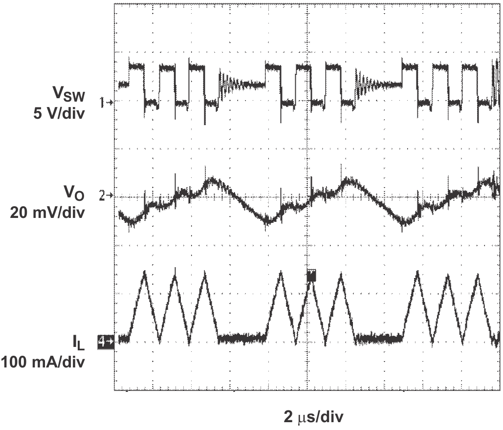
At light load currents, the device operates in power save mode, and the output voltage ripple is independent of the output capacitor value. The output voltage ripple is set by the internal comparator thresholds. The typical output voltage ripple is 1% of the output voltage Vo.
Table 3. Recommended Capacitors
| CAPACITOR VALUE | CASE SIZE | COMPONENT SUPPLIER | COMMENTS |
|---|---|---|---|
| 4.7 µF | 0805 | Taiyo Yuden JMK212BY475MG | Ceramic |
| 10 µF | 0805 | Taiyo Yuden JMK212BJ106MG TDK C12012X5ROJ106K |
Ceramic Ceramic |
| 10 µF | 1206 | Taiyo Yuden JMK316BJ106KL TDK C3216X5ROJ106M |
Ceramic |
| 22 µF | 1210 | Taiyo Yuden JMK325BJ226MM | Ceramic |
8.2.3 Application Curves
8.3 System Examples
8.3.1 Various Output Voltages
 Figure 16. Li-Ion to 1.8-V Fixed Output Voltage Version
 Figure 17. 1.8 V Fixed Output Voltage Version Using 4.7-µH Inductor
8.3.2 Adjustable Output Voltage Version Set to 1.5 V
 Figure 18. Adjustable Output Voltage Version Set to 1.5 V