SLVSB63A December 2011 – March 2016 TPS62231-Q1 , TPS622314-Q1
PRODUCTION DATA.
- 1 Features
- 2 Applications
- 3 Description
- 4 Revision History
- 5 pPin Configuration and Functions
- 6 Specifications
- 7 Detailed Description
- 8 Application and Implementation
- 9 Power Supply Recommendations
- 10Layout
- 11Device and Documentation Support
- 12Mechanical, Packaging, and Orderable Information
Package Options
Mechanical Data (Package|Pins)
- DRY|6
Thermal pad, mechanical data (Package|Pins)
- DRY|6
Orderable Information
6 Specifications
6.1 Absolute Maximum Ratings
over operating free-air temperature range (unless otherwise noted)(1)| MIN | MAX | UNIT | |||
|---|---|---|---|---|---|
| VI | Voltage at VIN and SW pin(2) | –0.3 | 7 | V | |
| Voltage at EN, MODE pin(2) | –0.3 | (VIN + 0.3) ≤7 | V | ||
| Voltage at FB pin(2) | –0.3 | 3.6 | V | ||
| Peak output current | internally limited | A | |||
| Power dissipation | Internally limited | ||||
| TJ | Maximum operating junction temperature | –40 | 125 | °C | |
| Tstg | Storage temperature | –65 | 150 | °C | |
(1) Stresses beyond those listed under Absolute Maximum Ratings may cause permanent damage to the device. These are stress ratings only, which do not imply functional operation of the device at these or any other conditions beyond those indicated under Recommended Operating Conditions. Exposure to absolute-maximum-rated conditions for extended periods may affect device reliability.
(2) All voltage values are with respect to network ground terminal.
6.2 ESD Ratings
| VALUE | UNIT | |||
|---|---|---|---|---|
| V(ESD) | Electrostatic discharge | Human-body model (HBM), per AEC Q100-002(1) | ±2000 | V |
| Charged-device model (CDM), per AEC Q100-011 | ±1000 | |||
| Machine Model (MM) | 200 | |||
(1) AEC Q100-002 indicates that HBM stressing shall be in accordance with the ANSI/ESDA/JEDEC JS-001 specification.
6.3 Recommended Operating Conditions
operating ambient temperature TA = –40 to 105°C (unless otherwise noted)(1)| MIN | NOM | MAX | UNIT | |||
|---|---|---|---|---|---|---|
| Supply voltage, VIN(4) | 2.05 | 6 | V | |||
| Effective output inductance | 0.7 | 1 or 2.2 | 4.3 | μH | ||
| Effective output capacitance | 2 | 4.7 | 15 | μF | ||
| Recommended minimum supply voltage | VOUT ≤ (VIN – 1 V)(2) | 500-mA maximum IOUT(3) | 3 | 3.6 | V | |
| 350-mA maximum IOUT(3) | 2.5 | 2.7 | ||||
| VOUT ≤ 1.8 V | 60-mA maximum output current(3) | 2.05 | ||||
| Operating junction temperature, TJ | –40 | 125 | °C | |||
| Ambient temperature, TA | –40 | 105 | °C | |||
(1) In applications where high power dissipation, poor package thermal resistance, or both are present, the maximum ambient temperature may have to be derated. Maximum ambient temperature (TA(max)) is dependent on the maximum operating junction temperature (TJ(max)), the maximum power dissipation of the device in the application (PD(max)), and the junction-to-ambient thermal resistance of the part/package in the application (RθJA), as given by the following equation: TA(max) = TJ(max) – (RθJA × PD(max)).
(2) For a voltage difference between minimum VIN and VOUT of ≥ 1 V
(3) Typical value applies for TA = 25°C, maximum value applies for TA = 105°C with TJ ≤ 125°C, PCB layout needs to support proper thermal performance.
(4) The minimum required supply voltage for start-up is 2.05 V. The device is functional down to the falling UVLO (undervoltage lockout) threshold.
6.4 Thermal Information
| THERMAL METRIC(1) | TPS62231x-Q1 | UNIT | |
|---|---|---|---|
| DRY (SON) | |||
| 6 PINS | |||
| RθJA | Junction-to-ambient thermal resistance | 294.5 | °C/W |
| RθJC(top) | Junction-to-case (top) thermal resistance | 166.5 | °C/W |
| RθJB | Junction-to-board thermal resistance | 166.1 | °C/W |
| ψJT | Junction-to-top characterization parameter | 27.3 | °C/W |
| ψJB | Junction-to-board characterization parameter | 159.9 | °C/W |
(1) For more information about traditional and new thermal metrics, see the Semiconductor and IC Package Thermal Metrics application report, SPRA953.
6.5 Electrical Characteristics
VIN = 3.6 V, VOUT = 1.8 V, EN = VIN, MODE = GND, TA = –40°C to 105°C(4), CIN = 2.2 μF, L = 2.2 μH, COUT = 4.7 μF, typical values are at TA = 25°C (unless otherwise noted).| PARAMETER | TEST CONDITIONS | MIN | TYP | MAX | UNIT | ||
|---|---|---|---|---|---|---|---|
| SUPPLY | |||||||
| VIN | Input voltage range(5) | 2.05 | 6 | V | |||
| IQ | Operating quiescent current | IOUT = 0 mA. PFM mode enabled (MODE = 0) device not switching |
22 | 40 | μA | ||
| IOUT = 0 mA. PFM mode enabled (MODE = 0) device switching, VIN = 3.6 V, VOUT = 1.2 V |
25 | μA | |||||
| IOUT = 0 mA. Switching with no load (MODE/DATA = VIN), PWM operation, VOUT = 1.8 V, L = 2.2 μH |
3 | mA | |||||
| ISD | Shutdown current | EN = GND(3) | 0.1 | 1 | μA | ||
| UVLO | Undervoltage-lockout threshold | Falling | 1.8 | 1.9 | V | ||
| Rising | 1.9 | 2.05 | V | ||||
| ENABLE, MODE THRESHOLD | |||||||
| VIH TH | Threshold for detecting high EN, MODE | 2.05 V ≤ VIN ≤ 6 V , rising edge | 0.8 | 1 | V | ||
| VIL TH HYS | Threshold for detecting low EN, MODE | 2.05 V ≤ VIN ≤ 6 V , falling edge | 0.4 | 0.6 | V | ||
| IIN | Input bias Current, EN, MODE | EN, MODE = GND or VIN = 3.6 V | 0.01 | 0.5 | μA | ||
| POWER SWITCH | |||||||
| RDS(ON) | High-side MOSFET on-resistance | VIN = 3.6 V, TJmax = 105°C; RDS(ON) max value | 600 | 850 | mΩ | ||
| Low-side MOSFET on-resistance | VIN = 3.6 V, TJmax = 105°C; RDS(ON) max value | 350 | 480 | ||||
| ILIMF | Forward current-limit MOSFET high side | VIN = 3.6 V, open loop | 690 | 850 | 1050 | mA | |
| Forward current-limit MOSFET low side | VIN = 3.6 V, open loop | 550 | 840 | 1220 | mA | ||
| TSD | Thermal shutdown | Increasing junction temperature | 150 | °C | |||
| Thermal shutdown hysteresis | Decreasing junction temperature | 20 | °C | ||||
| CONTROLLER | |||||||
| tONmin | Minimum on time | VIN = 3.6 V, VOUT = 1.8 V, Mode = high, IOUT = 0 mA | 135 | ns | |||
| tOFFmin | Minimum off time | 40 | ns | ||||
| OUTPUT | |||||||
| VREF | Internal reference voltage | 0.70 | V | ||||
| VOUT | Output voltage accuracy(1) | VIN = 3.6 V, Mode = GND, device operating in PFM Mode, IOUT = 0 mA | 0% | ||||
| VIN = 3.6 V, MODE = VIN, IOUT = 0 mA |
TA = 25°C | –2% | 2% | ||||
| TA = –40°C to 105°C | –2.5% | 2.5% | |||||
| DC output voltage load regulation | PWM operation, Mode = VIN = 3.6 V, VOUT = 1.8 V | 0.001 | %/mA | ||||
| DC output voltage line regulation | IOUT = 0 mA, Mode = VIN, 2.05 V ≤ VIN ≤ 6 V | 0 | %/V | ||||
| tStart | Start-up time | Time from active EN to VOUT = 1.8 V, VIN = 3.6 V, 10-Ω load |
100 | μs | |||
| ILK_SW | Leakage current into SW pin | VIN = VOUT = VSW = 3.6 V, EN = GND(2) | 0.1 | 0.5 | μA | ||
(1) VIN = VO + 1 V
(2) The internal resistor divider network is disconnected from FB pin.
(3) Shutdown current into VIN pin, includes internal leakage
(4) In applications where high power dissipation and/or poor package thermal resistance is present, the maximum ambient temperature may have to be derated. Maximum ambient temperature (TA(max)) is dependent on the maximum operating junction temperature (TJ(max)), the maximum power dissipation of the device in the application (PD(max)), and the junction-to-ambient thermal resistance of the part/package in the application (RθJA), as given by the following equation: TA(max) = TJ(max) – (RθJA × PD(max)).
(5) The minimum required supply voltage for start-up is 2.05 V. The device is functional down to the falling UVLO (undervoltage lockout) threshold
6.6 Typical Characteristics
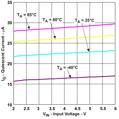
 Figure 1. Quiescent Current IQ vs Ambient Temperature (TA)
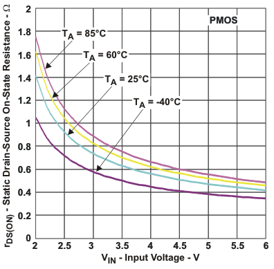
 Figure 3. PMOS RDS(ON) vs Supply Voltage VIN and Ambient Temperature (TA)
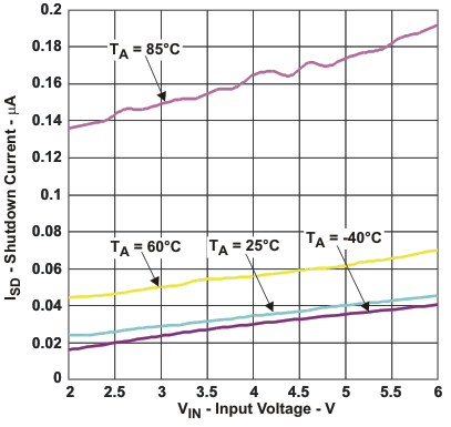
 Figure 2. Shutdown Current ISD vs Ambient Temperature (TA)
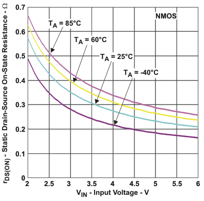
 Figure 4. NMOS RDS(ON) vs Supply Voltage VIN and Ambient Temperature (TA)