-
TPS6224x 2.25-MHz 300-mA Step-Down Converter in 2 x 2 WSON and SOT Package
- 1 Features
- 2 Applications
- 3 Description
- 4 Revision History
- 5 Device Options
- 6 Pin Configuration and Functions
- 7 Specifications
- 8 Detailed Description
- 9 Application and Implementation
- 10Power Supply Recommendations
- 11Layout
- 12Device and Documentation Support
- 13Mechanical, Packaging, and Orderable Information
- IMPORTANT NOTICE
Package Options
Mechanical Data (Package|Pins)
- DRV|6
Thermal pad, mechanical data (Package|Pins)
- DRV|6
Orderable Information
TPS6224x 2.25-MHz 300-mA Step-Down Converter in 2 x 2 WSON and SOT Package
1 Features
- High Efficiency - Greater Than 94%
- Output Current up to 300 mA
- VIN Range from 2 V to 6 V for Li-ion Batteries With Extended Voltage Range
- 2.25-MHz Fixed-Frequency Operation
- Power Save Mode at Light Load Currents
- Output Voltage Accuracy in PWM Mode ±1.5%
- Adjustable Output Voltage from 0.6 V to VIN
- Typical 15-μA Quiescent Current
- 100% Duty Cycle for Lowest Dropout
- Available in a SOT (5) and 2-mm × 2-mm × 0.8-mm WSON (6) Package
- Allows <1-mm Solution Height
2 Applications
- Bluetooth™ Headsets
- Mobile Phones, Smart Phones
- WLAN
- Low Power DSP Supplies
- Portable Media Players
- Digital Cameras
3 Description
The TPS6224x device is a highly efficient synchronous step-down DC-DC converter. The device provides up to 300-mA output current from a single Li-Ion cell and is ideal for battery powered portable applications like mobile phones and other portable equipment.
With an wide input voltage range of 2 V to 6 V, the device also supports two- and three-cell alkaline, 3.3-V and 5-V input voltage rails.
The TPS6224x operates at 2.25-MHz fixed switching frequency and enters power save mode operation at light load currents to maintain high efficiency over the entire load current range.
The power save mode is optimized for low output voltage ripple. For low-noise applications, the device can be forced into fixed-frequency pulse width modulation (PWM) mode by pulling the MODE pin high. In shutdown mode, the current consumption is reduced to less than 1 μA. The TPS6224x allows the use of small inductors and capacitors to achieve a small solution size.
The TPS6224x operates over a free-air temperature range of –40°C to 85°C. The device is available in a 5-pin SOT and a 6-pin 2-mm × 2-mm WSON package.
Device Information(1)
| PART NUMBER | PACKAGE | BODY SIZE (NOM) |
|---|---|---|
| TPS6224x | WSON (6) | 2.00 mm × 2.00 mm |
| SOT (5) | 2.90 mm × 1.60 mm |
- For all available packages, see the orderable addendum at the end of the data sheet.
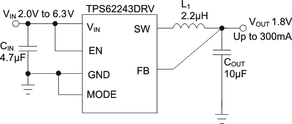
Typical Application Schematic

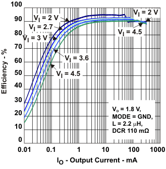
Efficiency vs Output Current

4 Revision History
Changes from B Revision (September 2007) to C Revision
- Changed editorial changes on bulletsGo
- Added ESD Ratings table, Feature Description section, Device Functional Modes, Application and Implementation section, Power Supply Recommendations section, Layout section, Device and Documentation Support section, and Mechanical, Packaging, and Orderable Information sectionGo
5 Device Options
| PART NUMBER (1) | OUTPUT VOLTAGE(2) |
|---|---|
| TPS62240 | adjustable |
| TPS62240 | adjustable |
| TPS62242 | 1.2 V fixed output voltage |
| TPS62243 | 1.8 V fixed output voltage |
6 Pin Configuration and Functions


Pin Functions
| PIN | I/O | DESCRIPTION | ||
|---|---|---|---|---|
| NAME | WSON | SOT | ||
| EN | 4 | 3 | I | This is the enable pin of the device. Pulling this pin to low forces the device into shutdown mode. Pulling this pin to high enables the device. This pin must be terminated. |
| GND | 6 | 2 | PWR | GND supply pin. |
| FB | 3 | 4 | I | Feedback pin for the internal regulation loop. Connect the external resistor divider to this pin. In case of fixed output voltage option, connect this pin directly to the output capacitor. |
| MODE | 2 | — | I | This pin is only available at WSON package option. MODE pin = High forces the device to operate in fixed-frequency PWM mode. MODE pin = Low enables the power save mode with automatic transition from PFM mode to fixed-frequency PWM mode. |
| SW | 1 | 5 | O | This is the switch pin and is connected to the internal MOSFET switches. Connect the inductor to this terminal. |
| VIN | 5 | 1 | PWR | VIN power supply pin. |
7 Specifications
7.1 Absolute Maximum Ratings
Over operating free-air temperature range (unless otherwise noted)(1)| MIN | MAX | UNIT | |||
|---|---|---|---|---|---|
| VIN | Input voltage (2) | –0.3 | 7 | V | |
| Voltage at EN, MODE | –0.3 | VIN +0.3, ≤7 | V | ||
| Voltage on SW | –0.3 | 7 | V | ||
| Peak output current | Internally limited | A | |||
| TJ | Maximum operating junction temperature | –40 | 125 | °C | |
| Tstg | Storage temperature | –65 | 150 | °C | |
7.2 ESD Ratings
| VALUE | UNIT | |||
|---|---|---|---|---|
| V(ESD) | Electrostatic discharge(3) | Human body model (HBM), per ANSI/ESDA/JEDEC JS-001, all pins(1) | ±2000 | V |
| Charged device model (CDM), per JEDEC specification JESD22-C101, all pins(2) | ±1000 | |||
7.3 Recommended Operating Conditions
Over operating free-air temperature range (unless otherwise noted)| MIN | NOM | MAX | UNIT | ||
|---|---|---|---|---|---|
| VIN | Supply voltage, VIN | 2 | 6 | V | |
| Output voltage for adjustable voltage | 0.6 | VIN | V | ||
| TA | Operating ambient temperature | –40 | 85 | °C | |
| TJ | Operating junction temperature | –40 | 125 | °C | |
7.4 Thermal Information
| THERMAL METRIC(1) | TPS6224x | UNIT | ||
|---|---|---|---|---|
| DRV [WSON] | DDC [SOT] | |||
| 6 PINS | 5 PINS | |||
| RθJA | Junction-to-ambient thermal resistance | 67.8 | 226.9 | °C/W |
| RθJC(top) | Junction-to-case (top) thermal resistance | 88.5 | 40.7 | °C/W |
| RθJB | Junction-to-board thermal resistance | 37.2 | 48.8 | °C/W |
| ψJT | Junction-to-top characterization parameter | 2.0 | 0.5 | °C/W |
| ψJB | Junction-to-board characterization parameter | 37.6 | 48.1 | °C/W |
| RθJC(bot) | Junction-to-case (bottom) thermal resistance | 7.9 | N/A | °C/W |
7.5 Electrical Characteristics
Over full operating ambient temperature range, typical values are at TA = 25°C. Unless otherwise noted, specifications apply for condition VIN = EN = 3.6 V. External components CIN = 4,7 μF 0603, COUT = 10 μF 0603, L = 2.2 μH, refer to parameter measurement information.| PARAMETER | TEST CONDITIONS | MIN | TYP | MAX | UNIT | |
|---|---|---|---|---|---|---|
| SUPPLY | ||||||
| VIN | Input voltage range | 2 | 6 | V | ||
| IOUT | Output current | 2.3 V ≤ VIN ≤ 6 V | 300 | mA | ||
| 2 V ≤ VIN ≤ 2.3 V | 150 | |||||
| IQ | Operating quiescent current | IOUT = 0 mA. PFM mode enabled (MODE = GND) device not switching | 15 | μA | ||
| IOUT = 0 mA. PFM mode enabled (MODE = GND) device switching, VOUT = 1.8 V, (1) | 18.5 | |||||
| IOUT = 0 mA, switching with no load (MODE = VIN), PWM operation , VOUT = 1.8 V, VIN = 3 V | 3.8 | mA | ||||
| ISD | Shutdown current | EN = GND | 0.1 | 1 | μA | |
| UVLO | Undervoltage lockout threshold | Falling | 1.85 | V | ||
| Rising | 1.95 | |||||
| ENABLE, MODE | ||||||
| VIH | High level input voltage, EN, MODE | 2 V ≤ VIN ≤ 6 V | 1 | VIN | V | |
| VIL | Low level input voltage, EN, MODE | 2 V ≤ VIN ≤ 6 V | 0 | 0.4 | V | |
| IIN | Input bias current, EN, MODE | EN, MODE = GND or VIN | 0.01 | 1 | μA | |
| POWER SWITCH | ||||||
| RDS(on) | High-side MOSFET ON-resistance | VIN = VGS = 3.6 V, TA = 25°C | 240 | 480 | mΩ | |
| Low-side MOSFET ON-resistance | 180 | 380 | ||||
| ILIMF | Forward current-limit MOSFET high-side and low-side | VIN = VGS = 3.6 V | 0.56 | 0.7 | 0.84 | A |
| TSD | Thermal shutdown | Increasing junction temperature | 140 | °C | ||
| Thermal shutdown hysteresis | Decreasing junction temperature | 20 | °C | |||
| OSCILLATOR | ||||||
| fSW | Oscillator frequency | 2 V ≤ VIN ≤ 6 V | 2 | 2.25 | 2.5 | MHz |
| OUTPUT | ||||||
| VOUT | Adjustable output voltage range | 0.6 | VIN | V | ||
| VREF | Reference voltage | 600 | mV | |||
| VFB | Feedback voltage | MODE = VIN, PWM operation, 2 V ≤ VIN ≤ 6 V, in fixed output voltage versions VFB = VOUT, see (3)
|
–1.5% | 0% | 1.5% | |
| Feedback voltage PFM mode | MODE = GND, device in PFM mode | 0% | ||||
| Load regulation | PWM mode | -0.5 | %/A | |||
| tStart Up | Start-up Time | Time from active EN to reach 95% of VOUT nominal | 500 | μs | ||
| tRamp | VOUT ramp-up time | Time to ramp from 5% to 95% of VOUT | 250 | μs | ||
| Ilkg | Leakage current into SW pin | VIN = 3.6 V, VIN = VOUT = VSW, EN = GND,(2) | 0.1 | 1 | μA | |
7.6 Typical Characteristics
 Figure 1. Shutdown Current Into VIN vs Input Voltage
 Figure 3. Static Drain-Source On-State Resistance vs Input Voltage
 Figure 2. Quiescent Current vs Input Voltage
 Figure 4. Static Drain-Source On-State Resistance vs Input Voltage