SLVSA67F February   2010  – April 2020 TPS62400-Q1 , TPS62402-Q1 , TPS62404-Q1 , TPS62405-Q1

UNLESS OTHERWISE NOTED, this document contains PRODUCTION DATA.  

  1. Features
  2. Applications
  3. Description
    1.     Device Images
      1.      Simplified Schematic
      2.      TPS62402-Q1 Efficiency versus Output Current, VOUT1 and VOUT2
  4. Revision History
  5. Device Comparison Table
  6. Pin Configuration and Functions
    1.     Pin Functions
  7. Specifications
    1. 7.1 Absolute Maximum Ratings
    2. 7.2 ESD Ratings
    3. 7.3 Recommended Operating Conditions
    4. 7.4 Thermal Information
    5. 7.5 Electrical Characteristics
    6. 7.6 Timing Requirements
    7. 7.7 Switching Characteristics
    8. 7.8 Typical Characteristics
  8. Parameter Measurement Information
  9. Detailed Description
    1. 9.1 Overview
      1. 9.1.1 Converter 1
      2. 9.1.2 Converter 2
    2. 9.2 Functional Block Diagram
    3. 9.3 Feature Description
      1. 9.3.1 Enable
      2. 9.3.2 DEF_1 Pin Function
      3. 9.3.3 180° Out-of-Phase Operation
      4. 9.3.4 Short-Circuit Protection
      5. 9.3.5 Thermal Shutdown
      6. 9.3.6 EasyScale Interface: One-Pin Serial Interface for Dynamic Output-Voltage Adjustment
        1. 9.3.6.1 General
        2. 9.3.6.2 Protocol
    4. 9.4 Device Functional Modes
      1. 9.4.1 Power-Save Mode
        1. 9.4.1.1 Dynamic Voltage Positioning
        2. 9.4.1.2 Soft Start
        3. 9.4.1.3 100% Duty-Cycle Low-Dropout Operation
        4. 9.4.1.4 Undervoltage Lockout
      2. 9.4.2 Mode Selection
    5. 9.5 Programming
      1. 9.5.1 Addressable Registers
        1. 9.5.1.1 Bit Decoding
        2. 9.5.1.2 Acknowledge
        3. 9.5.1.3 Mode Selection
  10. 10Application and Implementation
    1. 10.1 Application Information
    2. 10.2 Typical Application
      1. 10.2.1 Design Requirements
      2. 10.2.2 Detailed Design Procedure
        1. 10.2.2.1 Output Voltage Setting
          1. 10.2.2.1.1 Converter 1 Adjustable Default Output-Voltage Setting: TPS62400-Q1
          2. 10.2.2.1.2 Converter 1 Fixed Default Output-Voltage Setting (TPS62402-Q1, TPS62404-Q1, and TPS62405-Q1)
          3. 10.2.2.1.3 Converter 2 Adjustable Default Output-Voltage Setting (TPS62400-Q1):
          4. 10.2.2.1.4 Converter 2 Fixed Default Output-Voltage Setting
        2. 10.2.2.2 Output Filter Design (Inductor and Output Capacitor)
          1. 10.2.2.2.1 Inductor Selection
          2. 10.2.2.2.2 Output-Capacitor Selection
          3. 10.2.2.2.3 Input Capacitor Selection
      3. 10.2.3 Application Curves
    3. 10.3 System Examples
  11. 11Power Supply Recommendations
  12. 12Layout
    1. 12.1 Layout Guidelines
    2. 12.2 Layout Example
  13. 13Device and Documentation Support
    1. 13.1 Device Support
      1. 13.1.1 Third-Party Products Disclaimer
    2. 13.2 Related Links
    3. 13.3 Support Resources
    4. 13.4 Trademarks
    5. 13.5 Electrostatic Discharge Caution
    6. 13.6 Glossary
  14. 14Mechanical, Packaging, and Orderable Information

Package Options

Mechanical Data (Package|Pins)
Thermal pad, mechanical data (Package|Pins)
Orderable Information

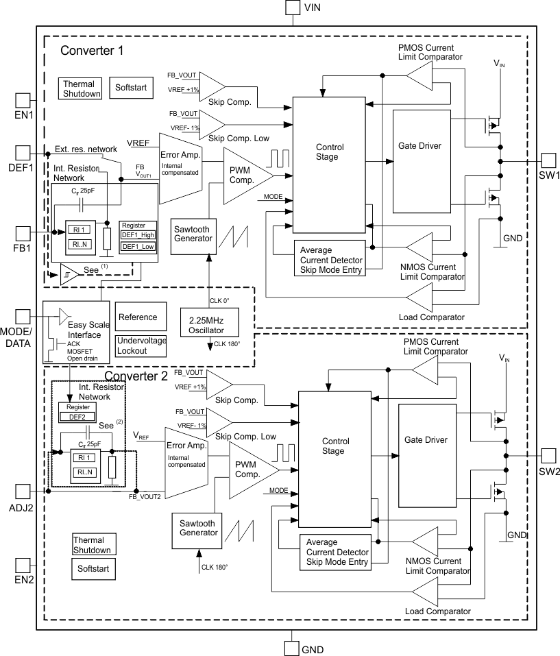
Functional Block Diagram

TPS62400-Q1 TPS62402-Q1 TPS62404-Q1 TPS62405-Q1 fbd_slvsa67.gif
In the fixed output-voltage version, the DEF_1 pin connects to an internal digital input and disconnects from the error amplifier.
To set the output voltage of converter 2 through the EasyScale™ interface, the ADJ2 pin must directly connect to VOUT2.